Meaning
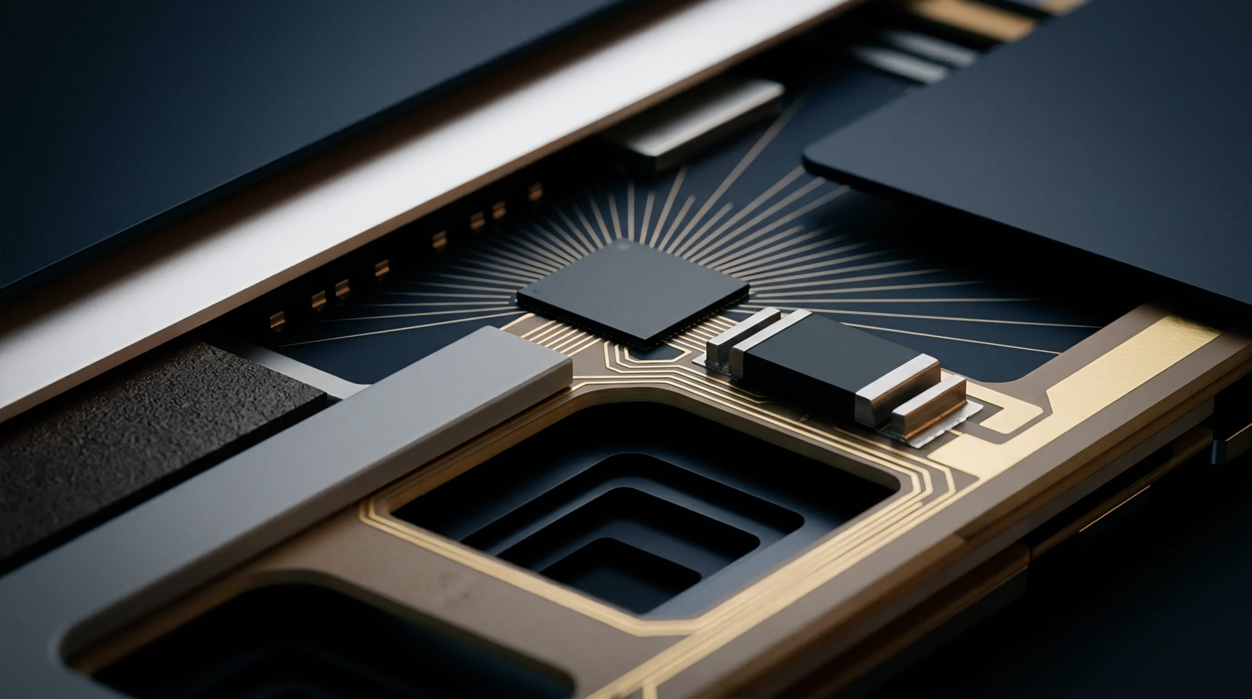
An internal copper architecture that delivers regulated electrical energy from board regulators to active silicon components is known as a power distribution network. This infrastructure governs current delivery across printed circuit boards while managing transient voltage drops during high frequency switching events. Operation stops at the die bump interface where local decoupling capacitance inside the semiconductor package begins filtering residual noise.
Thermal Dissipation
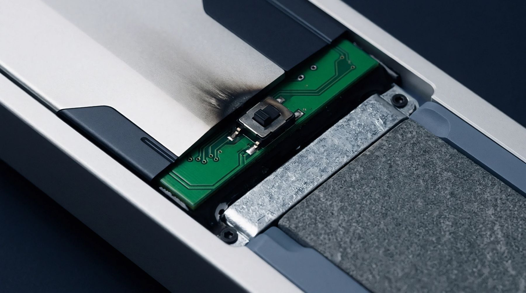
Copper trace routing generates parasitic resistance that turns supplied current directly into localized heat. Heat sinks attach directly above high current nodes to draw excess thermal energy away from delicate semiconductor junctions. Thermal resistance calculations dictate maximum allowable trace widths before component degradation occurs during continuous operation.
Voltage Regulation
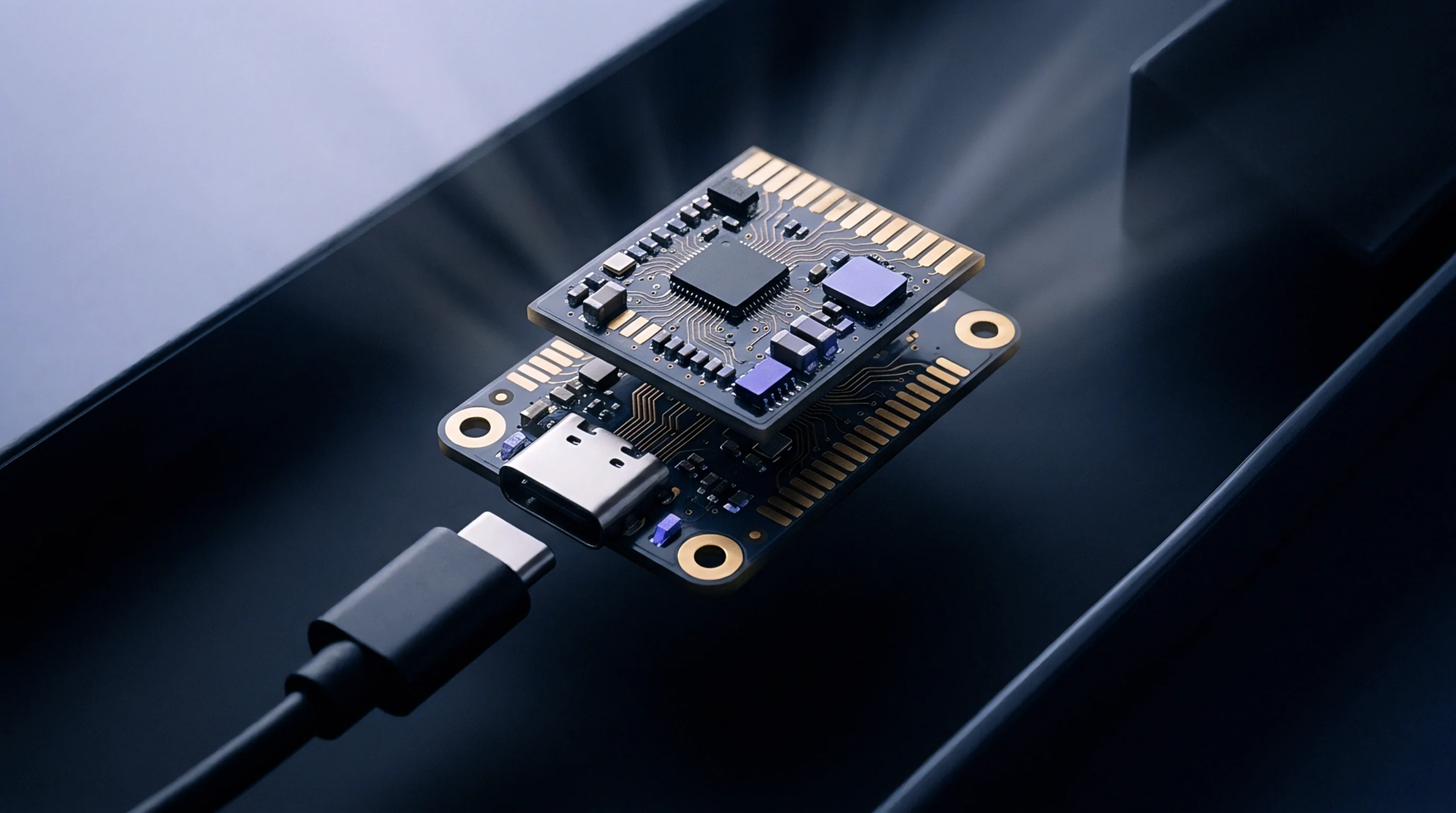
Current spikes across high speed processing units create instantaneous potential drops along the delivery path. Decoupling capacitors placed near active pins supply the charge needed to maintain steady voltage rails during sudden load transitions. Voltage margins shrink as semiconductor fabrication nodes decrease, forcing tighter tolerances on board level regulation modules.
Supplier Qualification
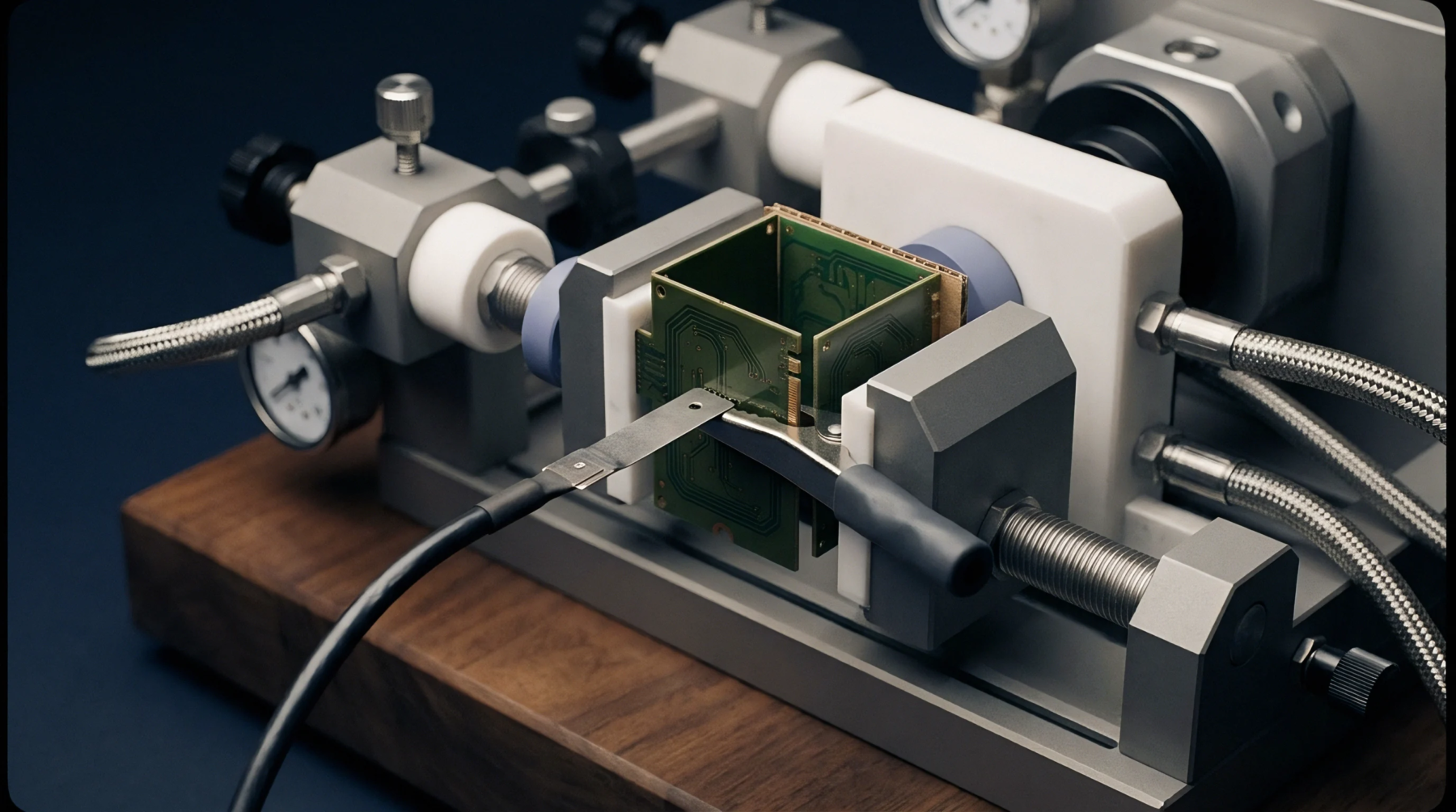
Manufacturers audit incoming copper laminates for purity levels and thickness uniformity before fabrication begins. Factory test fixtures measure transient response times across finished assemblies to verify compliance with electrical performance standards. Production sign off requires passing high current burn in tests that confirm solder joint integrity under maximum load conditions.