Decoupling Loop Inductance Minimization Protocols in Fine Pitch Array Layouts
Minimizing loop inductance in fine-pitch layouts requires microvia-in-pad placement, thin dielectric cores under 50 µm, and tight power-ground via coupling.
Loop
Transient current delivery in fine-pitch ICs depends on the physical geometry between die pads and storage capacitors. As pitch contracts from 0.8 mm down to 0.4 mm, tight spacing under the array restricts passive component land patterns, pushing decoupling capacitors out to the board perimeter or onto the back side. Total loop inductance scales directly with the area enclosed by this path ~ from the chip power pin through substrate microvias, across copper power and ground planes, down through breakout vias to the bypass capacitor body, and back along the ground return.
For high-density BGAs switching at multi-gigahertz frequencies, trace and via parasitic inductance dominates total power distribution network impedance. Once switching transients drop below a nanosecond, total loop series inductance matters far more than capacitance values, with each via operating as a parasitic loop inductor.

Total Inductance Path Breakdown in Fine Pitch Arrays
Calculating total loop inductance (Ltotal) requires isolating each physical segment of the AC current loop into five discrete components:
Ltotal = Lχppkg + Lviabreakout + Lplanespreading + Ltrace + Lcomponentesl
Breakout vias contribute the largest single fraction of loop inductance when capacitors are placed directly beneath the array on the bottom side of the board. A standard 0.4 mm long microvia pair adds roughly 100 pH to 250 pH of loop inductance, depending on via diameter, drill pitch, and proximity to the ground return.
| Loop Segment | Typical Dimension | Inductance Contribution (pH) | Percentage of Total Loop |
|---|---|---|---|
| Breakout Microvia Pair | 0.1 mm drill, 0.4 mm length | 120 – 220 | 35% – 45% |
| Component Body (0201 MLCC) | 0.6 mm x 0.3 mm pad size | 250 – 350 | 30% – 40% |
| Component Mounting Traces | 0.1 mm width, 0.2 mm length | 80 – 150 | 15% – 20% |
| Plane Spreading (10 µm core) | 0.05 mm dielectric separation | 20 – 50 | 5% – 10% |
| Data assumes four-layer microvia stack-up with surface-mounted 0201 multi-layer ceramic capacitors operating above 100 MHz. | |||
High Density Interconnect Geometry Constraints
Shrinking the ball pitch restricts available space for power escape routing. At 0.8 mm pitch, standard dog-bone routing provides dedicated vias for every power and ground ball. At 0.4 mm, tight clearances prevent running traces between pads, requiring via-in-pad plated-over microvias.
Impedance spikes trigger transient voltage droop: when PDN inductance exceeds design limits, sudden current draw during clock transitions pulls supply voltage below operating thresholds, causing logic errors in the silicon core.
Allowing total loop inductance to exceed target limits causes severe voltage ripple on core power rails, violating silicon operating tolerances.

Plane
Dielectric spacing between conductors governs field containment and parasitic spreading behavior in multi-layer stack-ups. Thin dielectrics keep spreading inductance low; when reference planes sit within 50 µm of power planes, magnetic flux cancellation between opposing current sheets suppresses parasitic inductance across the plane.
Spreading inductance (Lspread) represents the cavity’s resistance to rapid magnetic field expansion when a power ball draws high-frequency current, causing plane cavities to resonate at microwave frequencies.
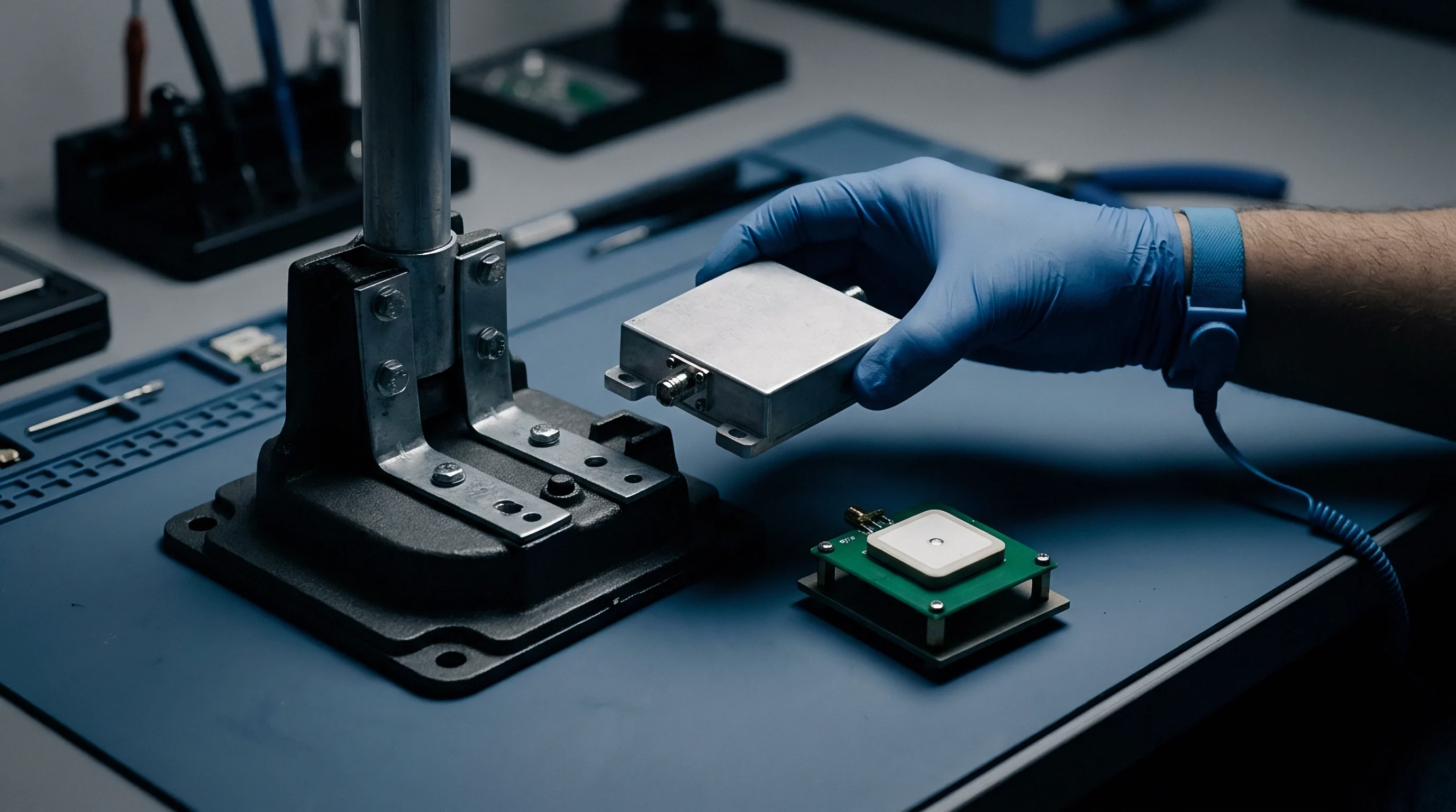
Dielectric Thickness and Spreading Behavior
Plane spreading inductance scales linearly with dielectric thickness and inversely with copper coverage density, following the relationship:
Lspread = fracμ0 · μr · dw
Where μ0 is the permeability of free space, μr is relative permeability, d is dielectric layer thickness, and w is effective wavefront width. Thinning the core dielectric from 100 µm down to 12 µm cuts spreading inductance eightfold between 100 MHz and 3 GHz.
Holding power distribution impedance below ten milliohms at one gigahertz requires dielectric core thicknesses under fifty micrometers between power and ground layers.

Microvia Stack Depth and Layer Assignment
Placing high-frequency decoupling planes near the surface keeps microvias short. Deeply buried power planes increase breakout via aspect ratio and length, adding up to 80 pH of loop inductance for each additional prepreg layer crossed.
Because microvias minimize physical height, standard sequential build-up stack-ups place primary power-ground plane pairs directly beneath microvia layers 1 ~ 2 or 2 ~ 3 to secure low-inductance return paths.
Fabrication variations alter dielectric thickness. To maintain target PDN impedance, IPC-6012 Class 3 sourcing agreements cap dielectric layer thickness variation at plus or minus ten percent.
Silicon
As passive components shrink, parasitic series limits move from ceramic bodies into substrate interconnects. Choosing bypass caps for fine-pitch arrays requires matching component equivalent series inductance (ESL) to board breakout capability ~ standard 0402 capacitors exhibit 500 pH to 800 pH of ESL, making them ineffective above 200 MHz.
Passive Component Architecture and Equivalent Series Inductance
Ultra-low ESL passives adjust internal electrode geometry to reduce parasitic magnetic fields. Reverse-geometry components ~ like 0306 MLCCs, where terminations run along the long edge ~ shorten the internal current path and drop ESL below 100 pH.
Multi-terminal land-side capacitors (such as X2Y architecture or eight-terminal interdigitated caps) establish parallel internal current paths that cancel mutual magnetic fields, damping noise and dropping effective component inductance below 50 pH.

Land Side Capacitor Integration for Sub Micron Arrays
Deep-trench silicon capacitors mounted inside the array footprint or embedded within the substrate deliver the lowest achievable loop inductance. Heights under 100 µm allow direct placement inside BGA cavity voids or on the substrate backside beneath solder balls.
Selecting sub-optimal passive package styles produces specific manufacturing and electrical failures across high-density assembly lines:
- Solder Voiding Under Substrate Pads occurs when microvia-in-pad structures lack proper copper capping, drawing solder away from 01005 passive terminations during reflow.
- Dielectric Crack Formation Under Thermal Cycling occurs when stiff ceramic bodies span regions of mismatched thermal expansion without compliant underfill.
- Resonant Frequency Misalignment Across Temperature occurs when Class 2 ceramic dielectrics lose effective capacitance at high DC bias voltages and elevated temperatures.
- Capacitance Derating Under DC Bias can reduce nominal decoupling capacity by up to sixty percent when small-case-size MLCCs operate near maximum rated voltage.
Transient voltage noise stems from both board layout choices and component ESL variations, though published package inductance ratings reflect ideal laboratory test fixtures rather than installed board conditions.
Pattern
The relative placement of breakout interconnects and bypass components dictates how effectively mutual flux cancellation reduces path impedance. Alternating power and ground vias in a checkerboard or side-by-side pattern maximizes loop overlap and field cancellation between opposing current vectors.
Via in Pad Placement for Inductance Cancellation
Placing microvias directly in array solder lands eliminates interconnect trace length, dropping trace inductance to zero pH and leaving only microvia barrel and plane spreading inductance in the loop.
When power and ground microvias sit at a center-to-center pitch of 0.4 mm, mutual inductance (M) cancels self-inductance (L1, L2) to lower total loop inductance according to:
Leffective = L1 + L2 – 2M
Tighter via pitch increases mutual coupling, suppressing total loop inductance.
Placing ground and power vias adjacent within a single pad land cancels mutual magnetic fields and suppresses transient inductance spikes.
How Does via Mutual Coupling Impact Decoupling Performance?
Consider an array breakout layout with two adjacent microvias at pitch s = 0.4 mm, length h = 0.3 mm, and drill radius r = 0.05 mm. Self-inductance for an isolated microvia is estimated using the standard cylindrical wire approximation:
Lvia = fracμ0 h2π left ≈ 185 pH
When driven with opposing currents, mutual inductance M between the pair subtracts from total loop inductance:
M = fracμ0 h2π left ≈ 82 pH
Net loop inductance for the pair drops from 370 pH to 206 pH ~ a forty-four percent reduction achieved entirely through geometric proximity and current alignment.
Accurate layout verification relies on explicit design rules within the EDA environment:
- Set minimum drill-to-copper clearances in design rule checks to accommodate via-in-pad microvia capture rings.
- Assign opposing current directions to adjacent via pairs within the array footprint.
- Map capacitor power terminals directly to ground via pairs to maximize mutual flux cancellation.
- Extract board parasitics with 3D electromagnetic field solvers before freezing production Gerber layers.
Unfilled microvias risk solder voiding, so engineering teams must verify whether board fabricators can reliably fill and cap microvias at 0.4 mm pitch without introducing surface planarization defects that harm assembly yield.

Outlay
Fabrication specifications for high-density PCBs balance NRE costs against achievable PDN impedance targets. Specifying thin buried dielectrics, filled via-in-pad microvias, and deep-trench silicon capacitors increases tooling and unit costs, demanding careful technical and financial evaluation during procurement.
Because high-frequency current paths are dominated by inductance, layout geometry directly governs power integrity, making explicit deliverable definitions essential in turnkey fabrication contracts.

Commercial Mechanics of High Density Stackups
Sequential build-up layers increase board cost non-linearly. Moving from a single-step microvia process (1-n-1) to a two-step sequential build-up (2-n-2) raises bare board cost by forty to sixty percent, with filled via-in-pad processing adding further fabrication overhead.
| Integration Scope | NRE Expense Range (USD) | Design Ownership | PDN Performance Verification Responsibility |
|---|---|---|---|
| Turnkey Reference Board | $5,000 – $15,000 | Factory owns layout databases | Factory guarantees baseline compliance |
| Semi-Custom Module | $20,000 – $45,000 | Shared database rights | Joint extraction and verification protocol |
| Custom HDI Substrate | $60,000 – $120,000+ | Buyer owns complete IPC-2581 package | Buyer verifies post-layout SI/PI models |
Deliverable Scope and Design Transfer Constraints
A thorough design transfer package avoids costly board respins caused by unverified layout changes, so contracts should specify required engineering deliverables before releasing tooling funds.
Omitting extracted S-parameter models from the design transfer package forces secondary NRE expenses for electromagnetic re-verification.
Verifying deliverables protects against unauthorized stack-up substitutions that degrade PDN performance:
- Native EDA Database Transfers provide layout geometry, constraint manager settings, and stack-up definitions in uncompiled, editable formats.
- Electromagnetic Simulation Extraction Models include Touchstone files (S-parameters) mapping power distribution network impedance up to 10 GHz.
- Fabrication Stackup Qualification Dossier specifies prepreg glass styles, resin percentages, and dielectric thickness tolerances for each copper layer.
- Production Acceptance Test Coupons place dedicated coupon structures on panel borders to check microvia barrel integrity and dielectric thickness after reflow.
Specifying low-inductance stack-up geometries without defining tight layer tolerances frequently leaves production lots failing to meet high-frequency impedance targets.