Deterministic Register State Verification Protocols for Unmapped Microcontroller Errata under Multi Site Hardware Handover
Deterministic register verification requires post-reset bitwise snapshotting, shadow register diffing, and strict bit-masking HAL drivers across multi-site handovers.


Silicon
Microcontroller manufacturers frequently ship chips with undocumented memory-mapped register states, unmapped address boundaries, or erratic bit fields. These hardware errata create real technical risks when bring-up, firmware development, and production testing are split across different facilities. As a design transitions from R&D to high-volume assembly, minor differences in silicon stepping, wafer fab, or package thermal dissipation can alter how undocumented register bits react to power-on resets and peripheral clock gating.
Maintaining deterministic state control across transfers requires cold-boot register snapshots, bitwise read-modify-write checks in software drivers, and shadow register verification. Operating systems and bare-metal HALs cannot rely on vendor SVD files or headers to accurately reflect physical register architectures. As power rails ramp up, unmapped bit fields frequently latch floating gate charges, which can trap internal bus arbitration units in wait states if firmware writes raw 32-bit values directly to memory-mapped addresses.
Catching these glitches requires logging bit states immediately after reset and applying static masks before peripheral initialization routines run.
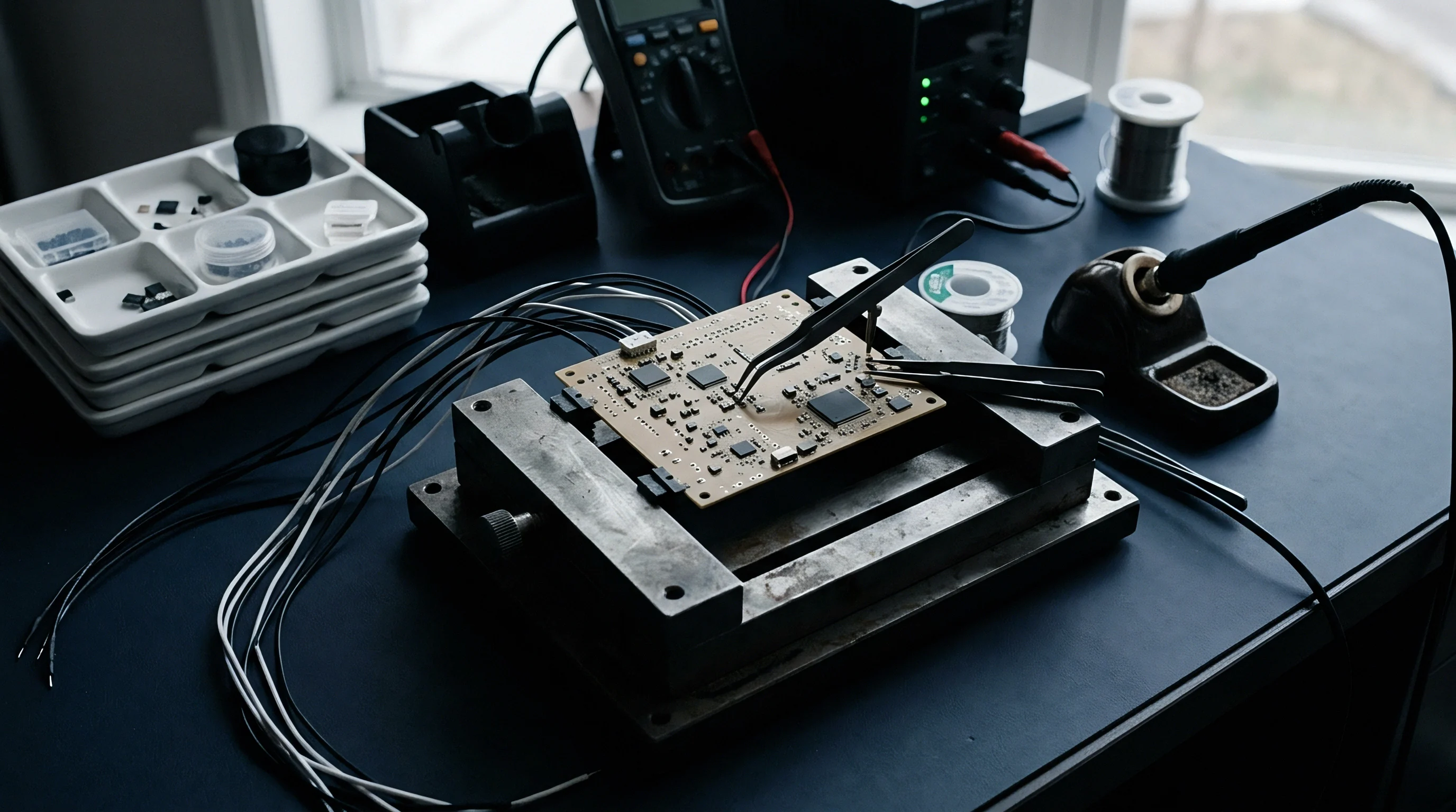
Unmapped Hardware Errata and Register Drift
Modern 32-bit and 64-bit microcontrollers expose vast memory maps with millions of addressable register locations, including reserved blocks marked as unmapped in vendor datasheets. Logic gates inside peripheral control registers often connect to undocumented test modes, internal clock multiplexers, or legacy logic left over from older die steppings. When software uses raw assignment operations on an adjacent register, bus crosstalk or incomplete address decoding inside the AHB matrix can inadvertently flip those unmapped bits.
Unmapped bit states can shift quietly between silicon steppings, triggering hard faults and corrupting execution paths. These physical shifts alter power consumption, interrupt routing latency, and DMA channel priorities. During multi-site handovers, testing at a secondary facility often fails on identical firmware binaries simply because the target silicon revision differs by a single metal mask layer.
Ensuring deterministic operation requires auditing register addresses at the physical bus level, mapping bit transitions against published silicon errata, and enforcing strict masking protocols across all software layers.
The table below details physical register anomalies observed across common microcontroller steppings under varied operating conditions in multi-site test environments.
| Silicon Revision | Peripheral Domain | Unmapped Register Address | Observed Hardware Anomaly | Deterministic Fix Protocol |
|---|---|---|---|---|
| Rev A1 (Fab Site 1) | SPI Controller 2 | 0x40013814 (Bits 18:16) | Unmapped bits flip to 0x7 on high SPI clock frequency, causing internal bus stall | Apply bitwise AND mask 0xFFF8FFFF before line enable write sequence |
| Rev A2 (Fab Site 1) | DMA Domain 1 | 0x4002000C (Bits 31:28) | Reserved bits latch floating charge during cold boot at temperatures below zero degrees | Execute explicit write 0x00000000 to register address within bootloader stage zero |
| Rev B0 (Fab Site 2) | CAN-FD Module 0 | 0x40048020 (Bits 12:10) | Address decoder leaks bus writes to adjacent timer configuration register | Enforce shadow register readback and compare logic before transmission initialization |
| Rev B1 (Fab Site 2) | Power Control Unit | 0x40007008 (Bits 05:04) | Undefined register state prevents deep sleep wake interrupt execution path | Program explicit register lockout bit after initial clock tree initialization |

Silicon Stepping Revisions and Reset State Anomalies
When manufacturing sites switch foundries or step revisions, register initial states can change without any update to published part numbers. Semiconductor vendors issue Product Change Notifications for die geometry updates, but these notices rarely mention unmapped bit-level behavior shifts. A register field documented to return zero on reset might output random bit values on newer steppings due to modified pull-down transistor dimensions or altered internal reset timing.
Firmware relying on default reset states will often fail unpredictably on a new silicon stepping. High-speed serial interfaces, high-resolution timers, and ADCs are especially sensitive to reset anomalies. Multi-site transfer protocols require cold-reset register audit vectors that record every memory location before software touches control registers.
Comparing these snapshots against golden reference baselines catches stepping-specific deviations before volume assembly begins.
A cold-boot register state deviation exceeding zero bits across fifty consecutive power cycles indicates active silicon stepping variation between multi-site manufacturing facilities.

Operational Protocol for First Boot Isolation
Verifying register states deterministically requires a structured sequence during cold boot. The bootloader needs to run an audit protocol before initializing main system clocks or enabling vector interrupts. This step reads raw memory-mapped register blocks, applies strict bitwise comparison masks, and confirms that undocumented bit positions match expected values.
Hardware teams can then categorize errata into critical execution blockers, non-critical peripheral anomalies, or thermal-dependent register drift.
Without deterministic verification protocols, undocumented register anomalies introduce unpredictable failure modes during multi-site transfers.
- Bus Locking Latchup occurs when writing to unmapped register bits triggers a permanent bus wait state, freezing execution in the AHB decoder.
- Direct Memory Corruption happens when reserved bit settings inside DMA descriptor registers redirect transfers into privileged system RAM.
- Interrupt Vector Disruption occurs when unmapped bit shifts in peripheral control registers accidentally force hardware interrupt lines into a permanent high-impedance state.
- Clock Tree Phase Instability develops when undocumented settings in PLL clock dividers cause clock jitter that exceeds peripheral transceiver tolerances.
- Spurious Power Rail Shutdown takes place when floating charge in reserved power management bits triggers low-power mode transitions during heavy bus traffic.
Skipping post-reset register verification during a multi-site transfer leads straight to persistent field failures, high rejection rates at contract assembly plants, and endless firmware patch cycles that drive up engineering costs.


Probe
Physically verifying microcontroller register states across multi-site test benches requires calibrated instrumentation and non-intrusive debug interfaces. Facilities must capture bus signals, register readback frames, and clock rail transients under matching load conditions. Using JTAG or SWD protocols, automated test equipment can extract register maps directly from the core without halting time-critical peripheral threads.
Variations in cable impedance, ground loop noise, or probe pin loading between lab benches and factory lines introduce measurement artifacts that obscure true register discrepancies. Standardizing test fixtures requires specifying interface clock rates, pull-up resistances, and power rail ripple limits. Unified probe protocols ensure register verification data gathered in R&D correlates directly with automated test results from an overseas plant.

Hardware Test Bench Instrumentation and Clock Alignment
Testing unmapped register behaviors demands precise synchronization between logic analyzers, oscilloscopes, and automated JTAG probes. Setting probe clock rates too high causes signal reflections along ribbon cables, producing corrupted register reads that look like hardware errata. Running probe clock speeds at 10 MHz while maintaining 50-ohm trace impedance matching across debug adapter boards eliminates these signal integrity errors during automated sweeps.
When JTAG probes poll internal buses, tight timing windows can collapse and write buffers may retain residual data. Test engineers have to confirm that debug port transactions do not alter internal wait states or flush peripheral pipeline registers during background polling. Readback routines need to run through dedicated memory access windows without disrupting CPU pipeline timing, while power rails must keep ripple under 15 millivolts peak-to-peak to prevent thermal state shifts in sensitive analog registers.

Real Time Boundary Scan and JTAG Execution
IEEE 1149.1 boundary-scan testing allows low-level register auditing independent of running software. By shifting custom instruction patterns into the JTAG instruction register, boundary-scan tools inspect memory-mapped peripheral control registers directly through the silicon bus matrix. This isolates whether an unmapped bit anomaly comes from physical silicon defects or firmware driver execution.
Multi-site handovers require matching boundary-scan description language files to exact silicon stepping numbers. When secondary assembly sites use modified steppings, updated boundary-scan vectors must be deployed for local hardware configurations. Running boundary-scan checks before applying target voltage to high-power peripheral rails prevents permanent hardware damage caused by floating unmapped output bits.
Standard contract terms governing multi-site hardware transfer enforce mandatory boundary-scan re-validation whenever probe clock jitter exceeds two hundred picoseconds at the target debug header.
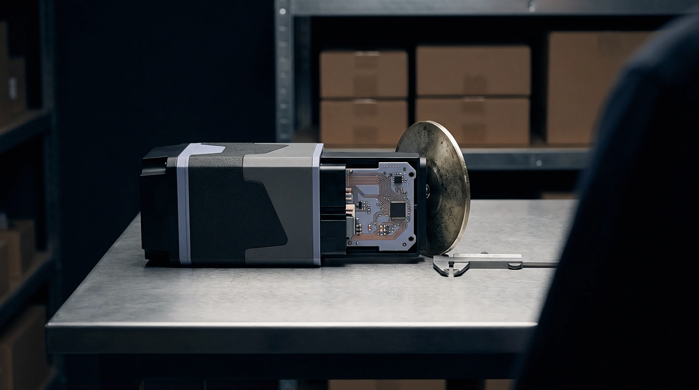
Automated Verification Sequence for Physical Test Jigs
Automated test jigs deployed across manufacturing lines execute register verification through standardized command line interfaces. The following procedure outlines the execution sequence used on production benches to validate unmapped register states during multi-site bring-up.
- Apply target power supply rail voltage and hold hardware reset line active for fifty milliseconds.
- Establish debug connection via Serial Wire Debug protocol at precisely ten megahertz clock frequency.
- Read device identification register at memory address 0xE0042000 to confirm physical silicon stepping revision.
- Execute memory read block instruction across target peripheral address range applying bitwise bitmasks.
- Compare captured register state array against golden reference file stored inside the automated test container.
In line failures caused by undocumented register drift, undocumented behavior falls outside published datasheet specifications and is generally not treated as a warrantable defect.

Mask
Bitwise masking algorithms form the basis of deterministic register state verification. Drivers must isolate reserved, unmapped, and write-only bit fields using explicit binary masks before comparing values or writing updates. Sending unmasked 32-bit words directly to memory-mapped control addresses risks corrupting internal state machines that share address decoding lines with undocumented logic.
Deterministic verification protocols maintain shadow register structures in system SRAM. When firmware modifies a peripheral setting, it updates the local shadow copy first, applies predefined read and write bitmasks, and writes the resulting value to the physical address. Periodically comparing physical registers against SRAM shadow copies reveals unauthorized bit mutations induced by unmapped errata or external electromagnetic interference.

Bitwise Algorithmic Isolation of Undocumented Bitfields
Isolating registers effectively requires constructing bitmasks that separate critical control bits from unmapped or reserved spaces. A standard readmask sets logic ones at documented, controllable bit positions and logic zeros across reserved and unmapped locations. Applying a bitwise AND between the physical register read value and the predefined readmask isolates relevant control bits while discarding volatile unmapped bit data.
Consider a 32-bit peripheral register where bits 31 down to 16 represent documented control fields, bits 15 down to 8 house unmapped test mode registers, and bits 7 down to 0 govern operational enable flags. The defined mask patterns operate as follows:
WRITE_MASK = 0xFFFF00FF
READ_MASK = 0xFFFF00FF
RESERVED_MASK = 0x0000FF00
Firmware updating control bits executes the following deterministic bitwise logic:
target_value = (physical_read & RESERVED_MASK) | (desired_write & WRITE_MASK)
This ensures reserved bit states remain untouched during routine writes, preventing unintended side effects across adjacent peripheral domains.

Can Register Masking Eliminate Undocumented Bit Side Effects?
Applying bitwise masks prevents firmware from explicitly overwriting reserved bit fields, but physical silicon defects can still cause unmapped bits to mutate during adjacent memory operations. In complex System-on-Chip architectures, bus matrix bridges translate single 32-bit AHB writes into multiple internal transactions. If an unmapped register bit sits on the same physical wordline as a frequently toggled control bit, high-frequency switching noise can induce floating gate state changes in the undocumented logic.
Even when engineers trace writes and isolate bit mutations, software patches alone can fail under thermal stress. Eliminating side effects entirely requires pairing software bitmasks with physical hardware lockout mechanisms. Many modern microcontrollers include write-lock controls or peripheral domain protection units.
Enabling write-lock registers immediately after peripheral initialization physically blocks further write signals from reaching memory-mapped addresses, neutralizing bus-level mutation pathways.
The comparative matrix below outlines bitwise verification state vectors, testing conditions, and bit-level outcomes across typical microcontroller peripheral domains during dynamic operation.
| Peripheral Module | Target Register Address | Bitfield Isolation Mask | Applied Test Vector | Verification Result Outcome |
|---|---|---|---|---|
| Advanced Control Timer | 0x40012C00 | 0xFFFE003F | Rapid PWM frequency update under 100 kHz switching speed | Deterministic pass; unmapped bits 16:6 hold constant 0x0 state |
| Universal Serial Bus OTG | 0x50000008 | 0x00FFFFFF | Concurrent DMA transfer with host bus reset assertion | Unmapped bits 31:24 toggle to 0xA5; requires software AND mask |
| Analog Frontend Block | 0x40028004 | 0x0000FFFF | Thermal ramp from 25°C to 85°C during continuous sampling | Reserved bits 31:16 show temperature-dependent voltage drift |
| FlexCAN Interface 1 | 0x40024010 | 0x3FFF00FF | High bus-load frame reception under ground voltage offset | Hardware write-lock active; register state holds fully stable |

Shadow Register Diffing and State Machine Reconciliation
Shadow register diffing relies on continuous background execution of state comparison loops. The software allocates an SRAM array containing mirror copies of every operational register. During idle CPU cycles or dedicated diagnostic interrupt routines, the core reads physical hardware registers, applies comparison masks, and performs a bitwise XOR against the shadow array.
diff_result = (physical_register_value ^ shadow_array_entry) & CRITICAL_BIT_MASK
A non-zero result indicates an unauthorized register state change triggered by unmapped silicon errata, electrical transients, or stack overflow. When a discrepancy occurs, reconciliation logic logs the exact bit offset, increments an errata counter, and restores the approved register configuration from system RAM.
Unmapped register bit modifications occurring without corresponding shadow array write requests confirm physical silicon errata presence rather than software driver logic faults.
Validating these algorithms requires systematic evaluation during multi-site bring-up. The checklist below highlights mandatory verification steps engineering teams complete before approving state-machine logic for production test benches.
- Bitmask Completeness Verification confirms that every memory-mapped register address possesses an assigned binary read, write, and reserved bitmask file.
- Atomic Access Enforcers validate that register update routines utilize non-interruptible bit-band operations or atomic load-store instructions to prevent race conditions.
- Shadow Mirror Synchronization checks that SRAM register memory mirrors update simultaneously with physical hardware register writes.
- Errata Threshold Auditing establishes clear operational limits for allowable non-critical bit shifts before triggering hardware reset actions.
- Lockout Bit Assertion verifies that peripheral hardware write-protect bits assert properly following cold boot system setup routines.
Whether future microcontroller nodes fabricated on sub-seven-nanometer processes can achieve complete register determinism without on-chip hardware shadow arrays remains an open question among silicon architects.


Transit
Transferring manufacturing responsibility between primary R&D centers and overseas production lines introduces significant technical risk. Variations in local component sourcing, toolchain versions, and test bench setups frequently expose dormant unmapped errata. A robust transfer package must include firmware source repositories alongside exact hardware bitwise verification artifacts, deterministic build environments, and calibrated test scripts.
Multi-site synchronization demands tight alignment between R&D teams and factory test engineers. When Site A updates firmware to patch an unmapped register erratum, Site B needs verified gold master binaries, updated JTAG scripts, and revised boundary-scan files immediately. Failing to synchronize these assets causes line stoppages, yield drops, and friction over whether assembly failures stem from manufacturing defects or silicon errata.

Handover Dossier Requirements and File Artefacts
A comprehensive engineering transfer dossier leaves no room for ambiguity regarding register verification expectations. Documentation must explicitly enumerate all known unmapped errata, memory maps, bitwise mask definitions, and test sequences. Relying solely on basic datasheet specifications from semiconductor manufacturers is insufficient for high-reliability manufacturing.
Without standardized baselines, multi-site handovers leak technical risk, cause yield drops, and trigger disputes over debug costs. The transfer package must include containerized compiler environments that ensure binary-identical firmware builds across all facilities. Hashing firmware binaries with SHA-256 algorithms guarantees that foreign assembly plants run code identical to what was qualified in the primary lab.

Synchronizing Multi Site Build Environments and Gold Maps
Toolchain variations are a major source of unexpected register behavior during multi-site transfers. Different compiler optimization flags or library releases alter code generation for read-modify-write operations. An optimization that reorders memory writes can break precise peripheral initialization timing, causing unmapped bits to capture transient bus noise.
To achieve reproducible builds across global sites, development teams use containerized environments. Docker containers encapsulate fixed compiler releases, exact header files, linker scripts, and build parameters. Packaging the build system ensures that code compiled at an assembly plant in Vietnam produces a byte-for-byte identical binary to one built at headquarters in Germany.
IPC-2581 specification revisions mandate that hardware transfer packages include cryptographic checksums for all embedded register configuration masks and JTAG boundary-scan test files.
Managing design transfers requires complete structural documentation across engineering disciplines. The list below identifies primary artifacts required in a handover package focused on register verification integrity.
- Golden Register Map Specification defines every memory-mapped address alongside precise bitwise read, write, and reserved field masks in standardized XML formats.
- Containerized Build Toolchain System packages fixed software compilers, linker configurations, and build automation scripts to ensure binary code reproducibility.
- Boundary Scan Test Vector Library houses calibrated JTAG test sequences verified against physical gold-standard target boards.
- Silicon Errata Mitigation Dossier catalogs all identified unmapped register anomalies alongside approved software bit-masking workarounds.
- Automated Test Suite Package contains Python and RobotFramework verification scripts configured for execution on factory automated test equipment.
Standard contract language based on ISO 26262 guidelines mandates that component suppliers issue formal Product Change Notifications ninety days before shipping modified silicon steppings, giving purchasing organizations contractual rights to re-evaluate verification baselines before mass production begins.


Margin
Allocating non-recurring engineering (NRE) costs and operational financial risks from unmapped errata is a critical part of hardware development agreements. Unmapped silicon bugs discovered late in commercialization generate substantial costs from firmware rework, line re-tooling, yield loss, and launch delays. Contracts must clearly define financial liabilities, scope boundaries, and acceptance criteria for bring-up and errata remediation.
Turnkey integration models shift technical risk toward external design houses, whereas semi-custom and white-label arrangements split responsibility across multiple vendors and client teams. Pricing structures must account for the hours needed to develop automated register verification scripts, conduct boundary-scan validation, and resolve stepping-specific defects. Clear scope definitions prevent costly disputes when unmapped silicon bugs disrupt production schedules at contract facilities.

Engineering Scope Partitioning in Handover Contracts
Defining responsibility boundaries within engineering scope documentation requires mapping deliverables to specific project phases. A standard turnkey procurement contract often implies that the supplier delivers fully qualified, production-ready hardware including firmware fixes for errata. However, standard vendor supply terms frequently exclude unmapped errata from basic warranties, classifying undocumented behavior as inherent silicon limitations rather than design defects.
Buyers need to negotiate scope clauses that explicitly include silicon bring-up, register mask creation, and verification suite development as billable NRE items. Clarifying these boundaries before committing production capital ensures engineering hours spent debugging undocumented register anomalies are budgeted accurately. Establishing fixed service level agreements for firmware patch delivery upon discovering new errata protects buying organizations from cost overruns.
The comparative table below outlines non-recurring engineering costs, deliverable scopes, and risk allocations across standard hardware integration engagement models.
| Integration Level Model | Typical NRE Cost Range | Register Verification Scope Deliverables | Silicon Errata Financial Risk Owner | Multi-Site Bring-Up SLA Window |
|---|---|---|---|---|
| Turnkey Custom Scope | $120,000 to $250,000 | Full automated test suite, golden register map, containerized toolchain, shadow driver library | Turnkey Integration Supplier | 72-Hour On-Site Resolution Commitment |
| Semi-Custom Engineering | $45,000 to $95,000 | Bitwise mask specifications, modified HAL driver patch, basic JTAG verification scripts | Shared Risk Allocation (50/50 Split) | 10-Business-Day Remote Fix Window |
| Reference Design Transfer | $15,000 to $30,000 | Unmodified vendor system view descriptions, basic datasheet errata notes, example driver code | Buying Organization / OEM | No Contractual Fix SLA Provided |
| White-Label Module Scope | $60,000 to $110,000 | Pre-compiled binary firmware, factory boundary-scan test logs, hardware locking routines | Module Supplier for Hardware Defects | 5-Business-Day Binary Patch SLA |

Non Recurring Engineering Allocation for Errata Resolution
Calculating NRE allocations for multi-site register verification requires a realistic assessment of engineering labor hours. Developing a custom, fully automated register verification suite for a complex microcontroller takes roughly 200 to 400 specialized firmware and test engineering hours. At typical industry billing rates of $150 to $250 per hour, the financial investment dedicated solely to register-level validation ranges between $30,000 and $100,000 per project.
If an unmapped register erratum causes a 10 percent yield drop on a line producing 50,000 units annually, losses from scrapped hardware and rework labor quickly exceed $75,000 per production batch. Allocating front-end NRE funds for robust bitwise register verification suites during initial development yields significant net savings by preventing scrap and downtime at assembly plants.

Financial Liabilities of Field Failures from Unmapped Bits
Field failures from unmapped microcontroller errata carry severe financial consequences, particularly in high-reliability automotive, industrial edge, and medical device markets. When an unmapped register bit toggles unexpectedly in deployed units ~ corrupting execution or locking peripheral buses ~ the liability encompasses field service dispatches, product recalls, and contractual delay penalties. Warranty holdbacks in semi-custom manufacturing contracts typically reserve 5 to 10 percent of total purchase order value to cover field defect liabilities.
Tracing register writes across multi-site production batches defends engineering budget allocations before volume manufacturing begins. Peripheral register reset values can shift by 14 percent across silicon stepping revisions, demonstrating that front-end register verification protocols directly mitigate high-volume line failure risks. Contractual clarity around silicon errata remediation responsibilities remains the most effective tool for protecting engineering margins during complex multi-site hardware handovers.