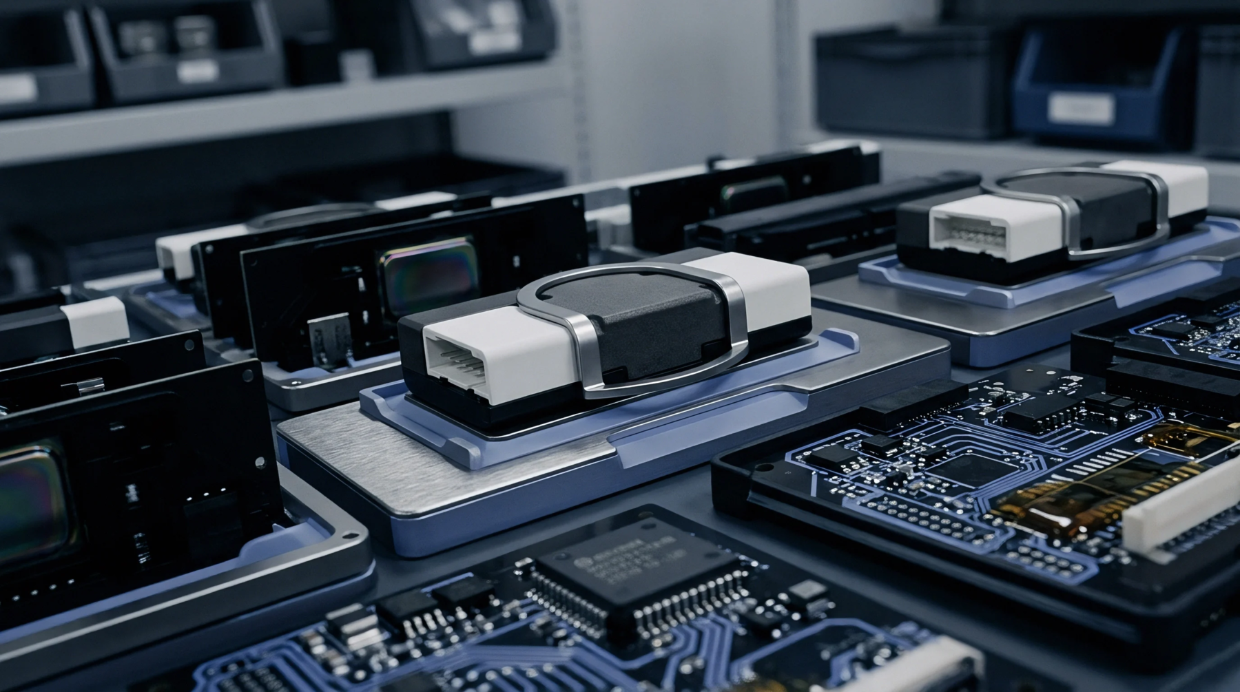
Managing Cross Fabricator Stack up Equivalence in High Frequency Wireless Boards
Managing cross-fabricator high-frequency stack-up equivalence requires controlling copper surface roughness, glass weave pitch, and press cured height tolerances.
Managing cross-fabricator high-frequency stack-up equivalence requires controlling copper surface roughness, glass weave pitch, and press cured height tolerances.

Continuous buffer auditing and strict milestone-linked escrow arbitrate working capital drag while insulating multi-tier supply lines from latent defect costs.

Matching transfer stackups across suppliers requires harmonizing trace undercut factors, glass style selections, and coupon measurement baselines.

Embedded silicon capacitors suppress packaging parasitics when cavity loop inductance stays below 10 pH and co-design balances damping against yield risk.
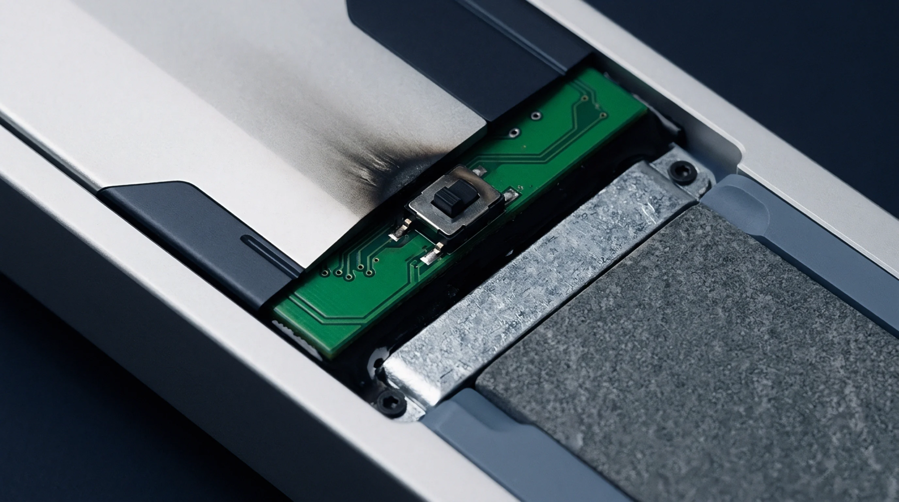
Rigorous RF substrate selection pairs tight dielectric tolerances with symmetric CTE stack-ups to prevent phase detuning and solder joint fatigue failure.
Laminate thickness collapse from uncontrolled resin flow forces costly radio recertification, shifting liability to fabricators only under strict RF covenants.
Transferring hardware across tiers succeeds only when native CAD constraints, containerized firmware builds, and custom test tooling stay under buyer custody.
Substrate dielectric variance alters trace capacitance and phase velocity, driving high-frequency impedance offsets, skew, and eye-closure failures.

Designing automated contact interface boards for high-volume semiconductor testing requires balancing pin wiping mechanics, high-frequency signal integrity, and mechanical stiffener design to prevent substrate deflection under multi-hundred-kilogram contactor loads.

Establishing hardware and firmware transfer rights demands uncompiled source code, raw layout schematics, build containers, and verified test fixtures.

Minimizing loop inductance in fine-pitch layouts requires microvia-in-pad placement, thin dielectric cores under 50 µm, and tight power-ground via coupling.

Unbundling engineering deliverables separates physical component supply from native design files, firmware repositories, and test fixtures, ensuring dual-sourcing rights and transparent landed costs.

Substrate dielectric tolerance and etch variance shift trace impedance, raising return loss and degrading RF power amplifier efficiency in custom module designs.
Expertise is a utility, not a secret. sentiention™ publishes its working knowledge as open reference: intelligence layer covering the materials it sources, the markets it enters, and the reference that serves both.