
Interconnect Pin Allocation and Plane Isolation in Semi Custom Modules
Optimize semi-custom module pinouts by interleaving ground lines and isolating power planes to prevent crosstalk and maintain target return path integrity.
Optimize semi-custom module pinouts by interleaving ground lines and isolating power planes to prevent crosstalk and maintain target return path integrity.

Allocate dedicated return pins for high-speed lines to minimize loop inductance, ground bounce, and costly tooling revisions across custom interfaces.
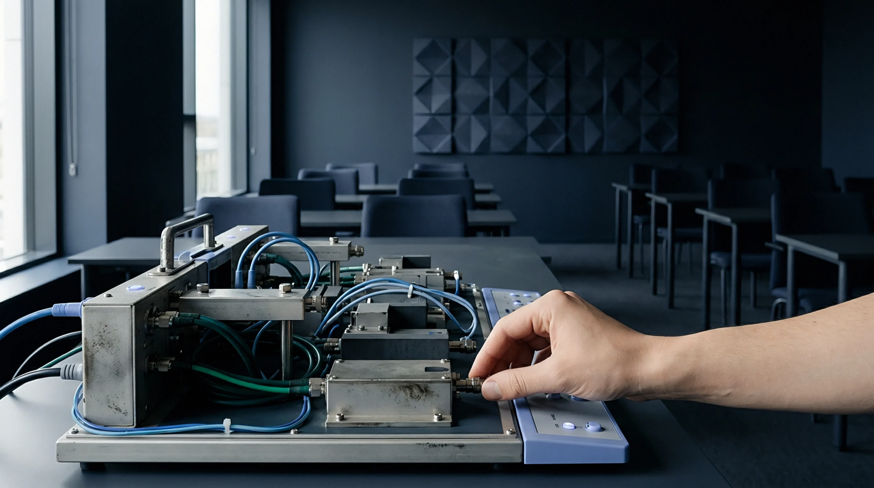
Modeling parasitic inductance during optical die shrink transitions prevents high-frequency peaking, preserves eye linearity, and controls module re-tooling costs.
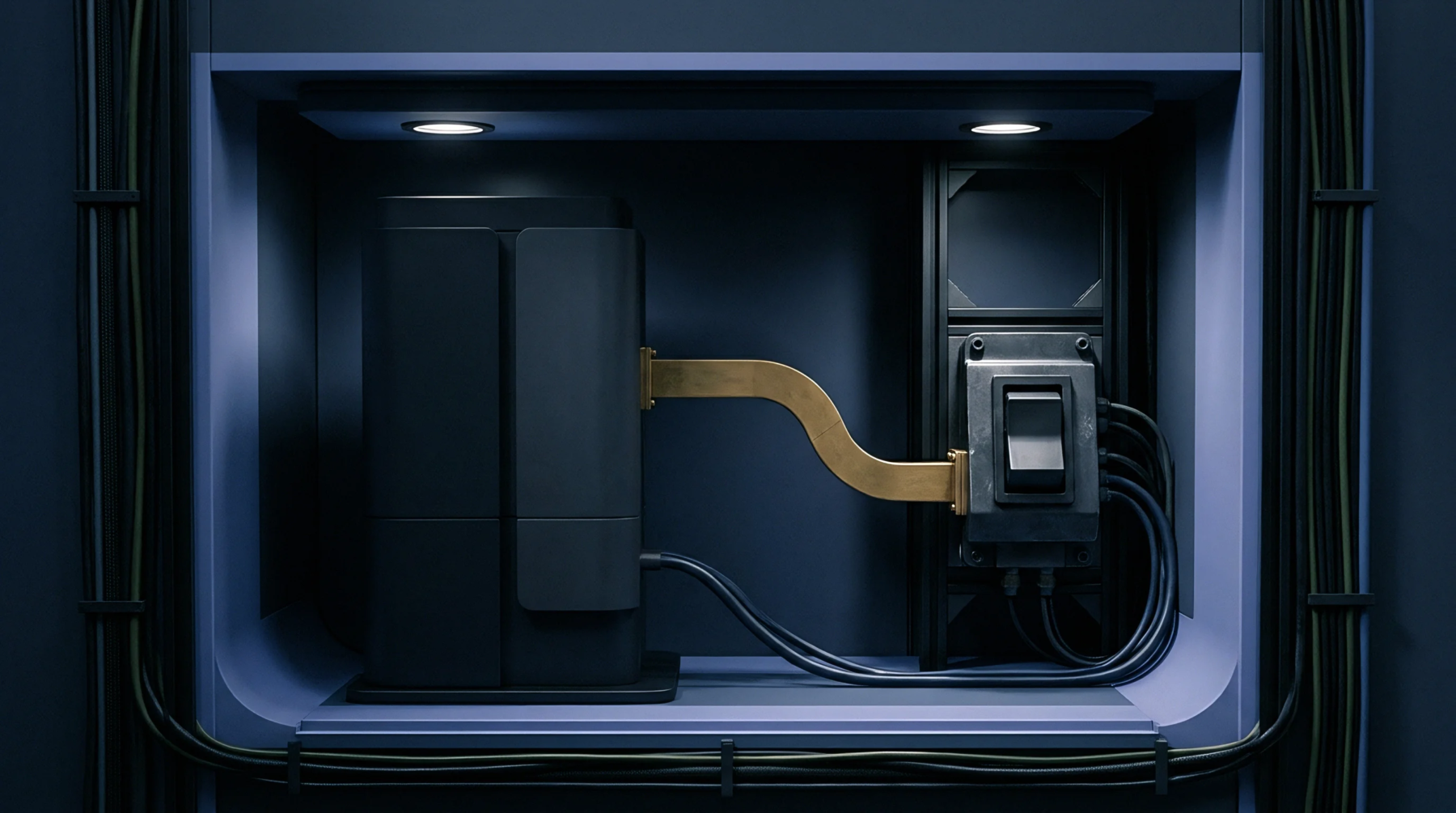
Sub-3nm transceiver power network noise requires target impedance below 10 milliohms up to 20 GHz to prevent supply-ripple-induced jitter failures.

Escrow test fixture builds fail verification when unrecorded floor edits shift pogo pin inductance or calibration matrices past standard threshold limits.
Mounting capacitors directly on the package backside using filled microvias cuts loop inductance below twenty picohenries and safeguards transient supply rails.
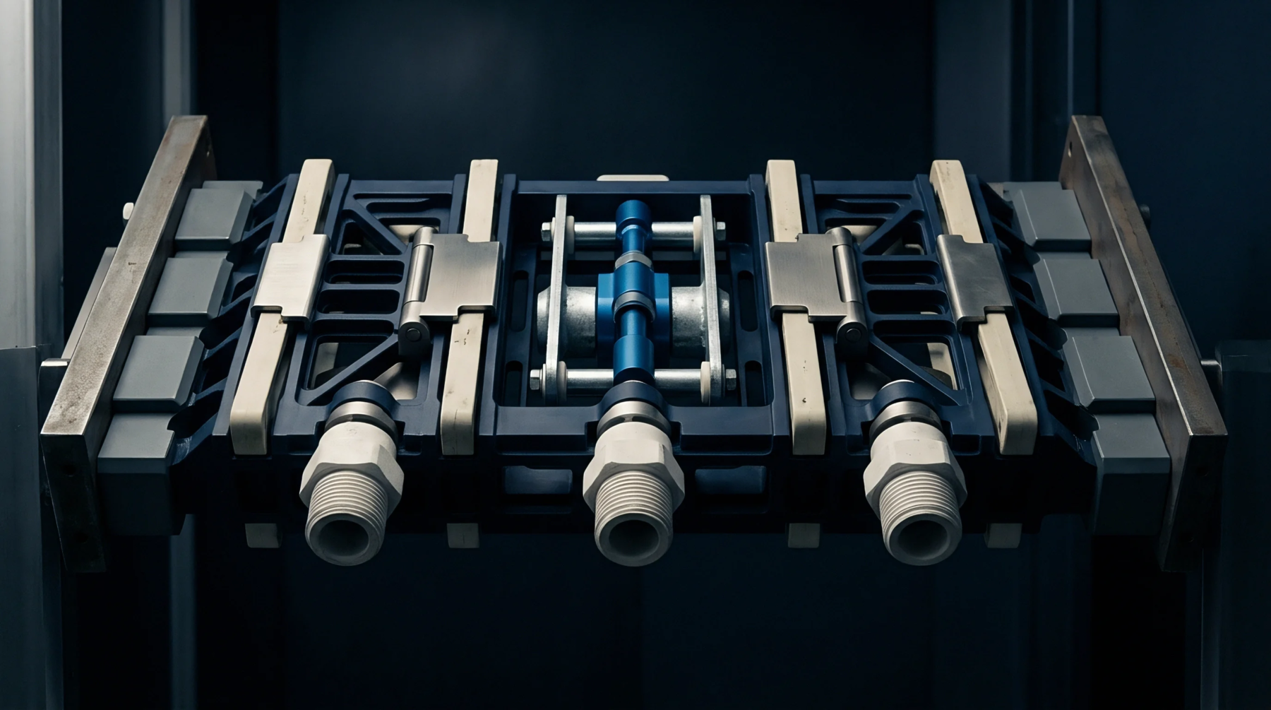
Mechanical fatigue in test contactor plungers diverts high-frequency currents into internal springs, inflating parasitic inductance and triggering false scrap.
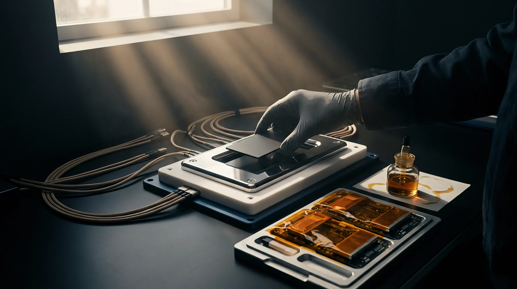
Initial contact resistance verification isolates test socket wear to prevent false radio parametric failures and secure accurate module production yields.
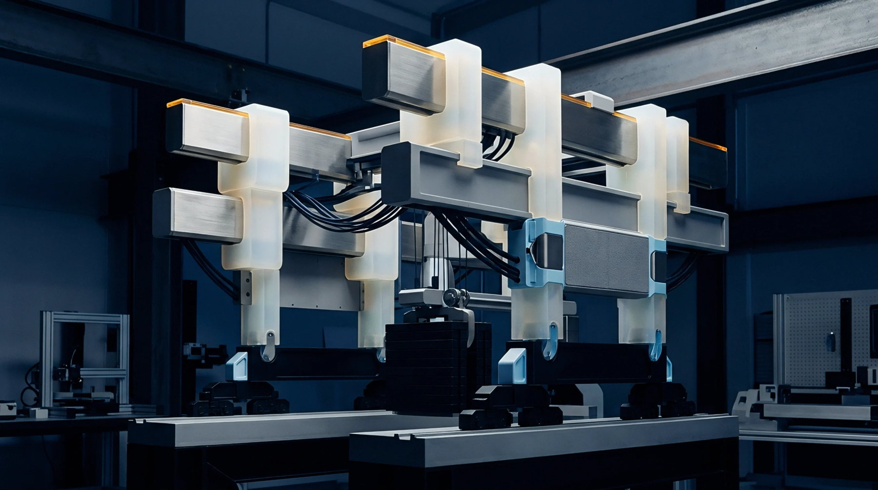
Ground allocation liability across hardware integration tiers requires explicit interface control documents defining return path impedances and chassis bonds.
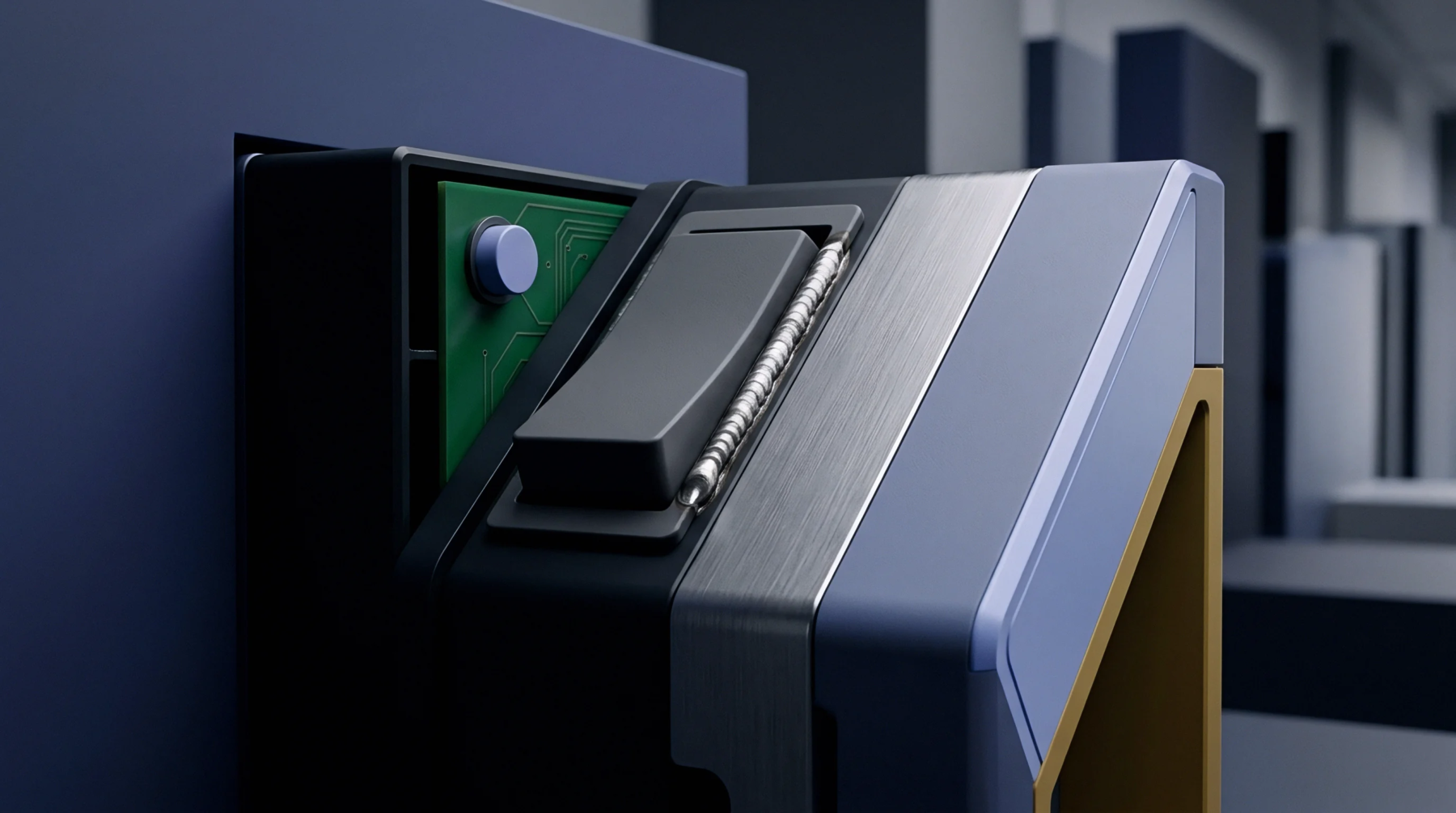
Die shrink equivalence demands full 3D electromagnetic loop extraction to prevent high-frequency current loop displacements from causing transient rail failures.
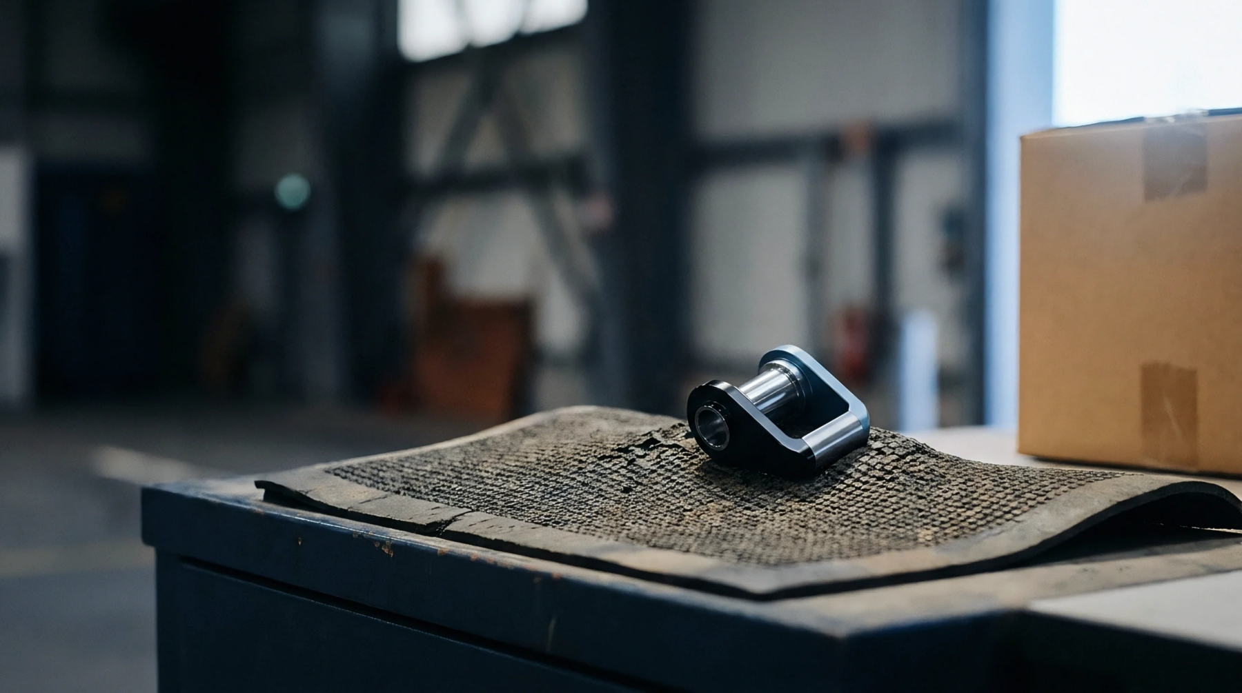
Extracting structural defect models for modified surface mount nets maps parasitic RLC shifts to maintain signal integrity and structural test coverage.
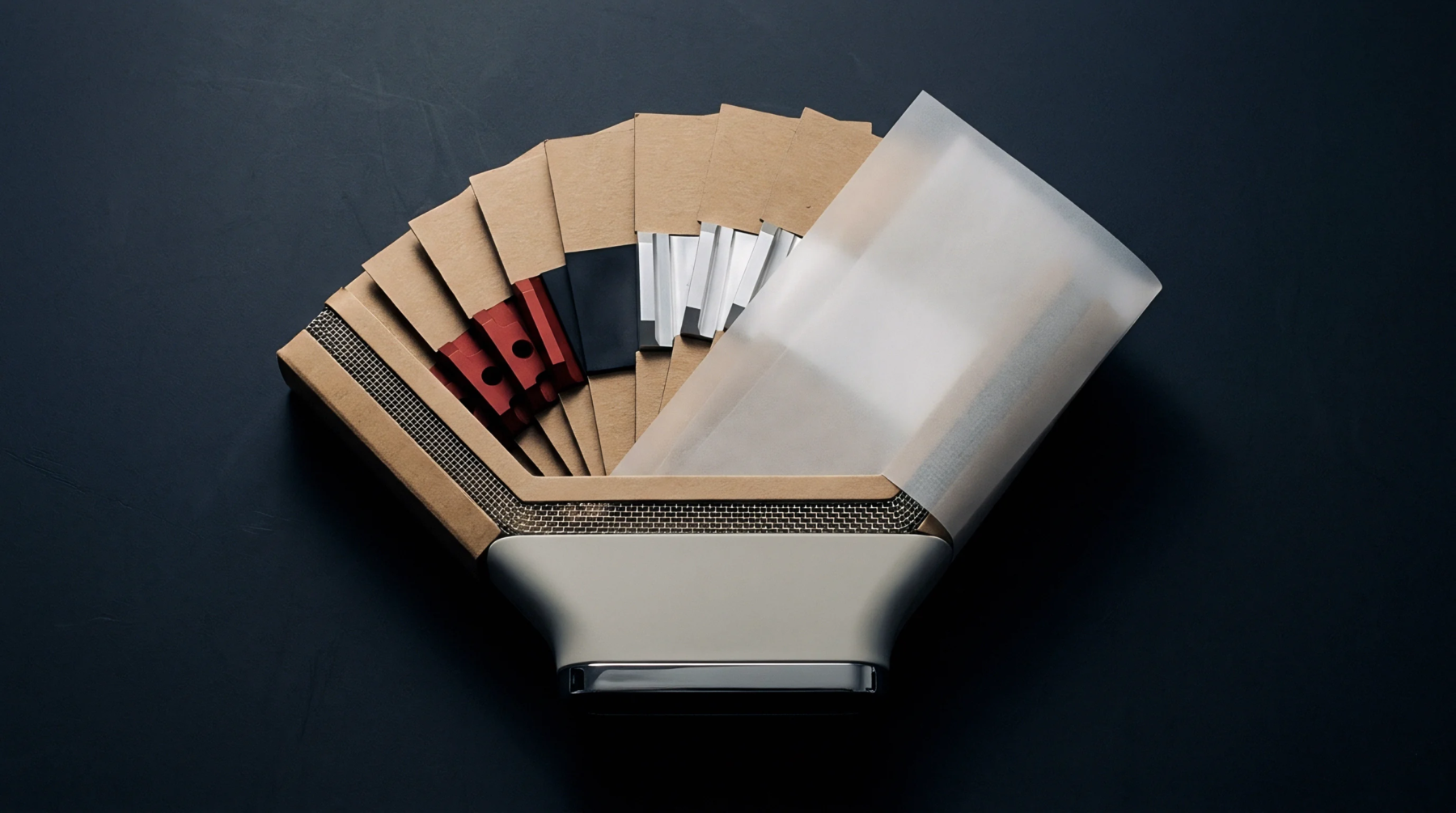
Minimizing loop inductance in fine-pitch layouts requires microvia-in-pad placement, thin dielectric cores under 50 µm, and tight power-ground via coupling.
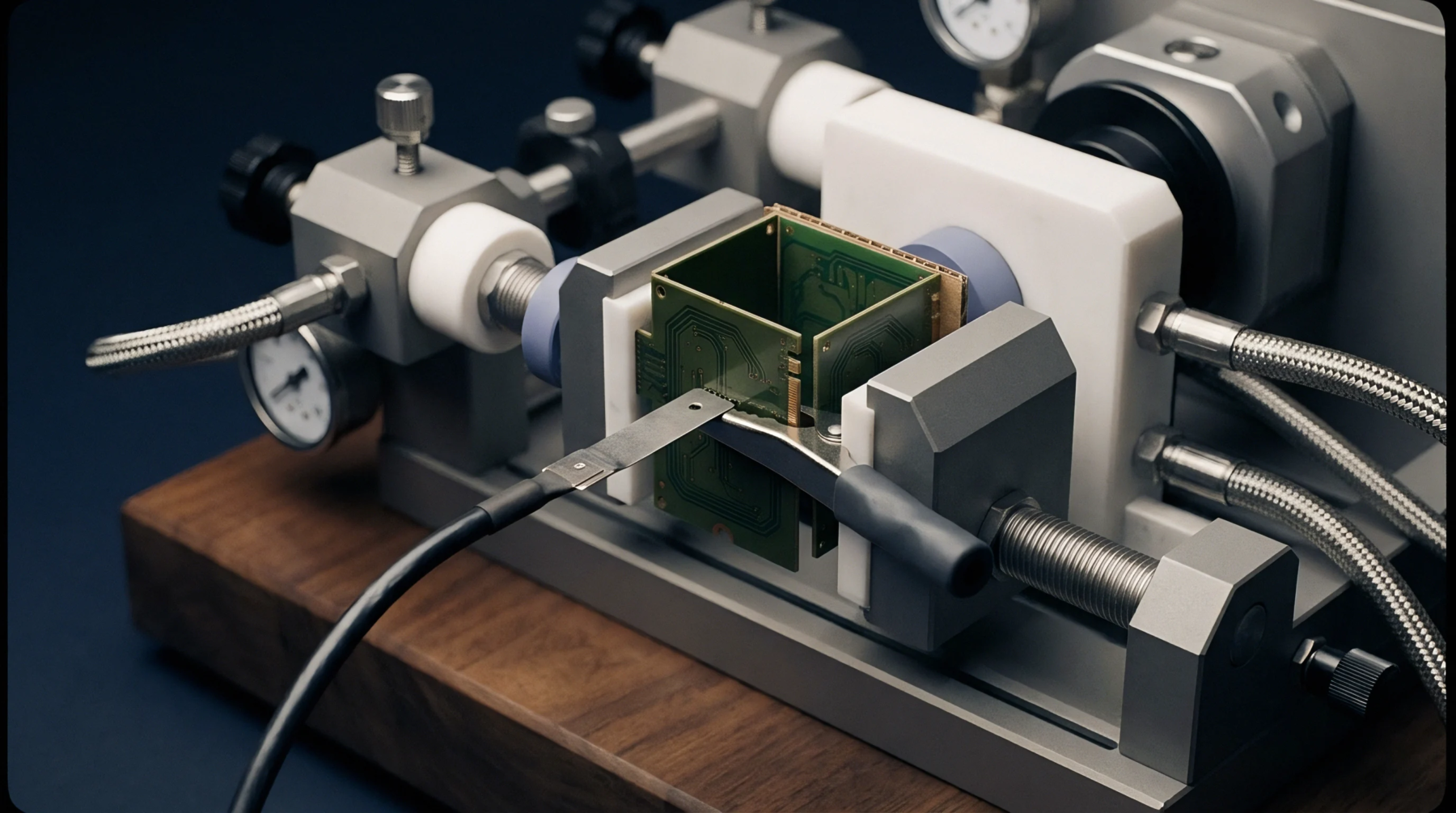
Silicon die shrinks accelerate output driver edge rates and elevate parasitic inductance, requiring full signal integrity auditing and updated IBIS models before drop-in assembly signoff.
Expertise is a utility, not a secret. sentiention™ publishes its working knowledge as open reference: intelligence layer covering the materials it sources, the markets it enters, and the reference that serves both.