Automated Hardware in the Loop Bus Stress Testing for Microcontrollers
Automated HIL bus stress testing requires nanosecond FPGA signal injection to prove microcontroller software timing and bus off recovery margins under real physical layer corruption.


Probe
Automated test benches interface directly with microcontroller physical pins through calibrated signal injection nodes. Designing these electrical connections demands exact matching of trace impedance, dynamic capacitive loading, and analog switch bandwidth. A standard microcontroller evaluation board exposes general-purpose input and output pins alongside dedicated Controller Area Network, Serial Peripheral Interface, and Inter-Integrated Circuit bus transceivers.
Stress rigs tap these lines using high-bandwidth field-effect transistor switches and solid-state multiplexers to insert physical layer anomalies without introducing parasitic attenuation during nominal pass-through operation.
Signal injection nodes must remain electrically transparent during baseline monitoring. Connecting external pulse generators or variable load banks directly introduces stub capacitance, and stubs longer than ten millimeters distort rising edge transitions on high-speed buses like Controller Area Network Flexible Data-Rate running at five megabits per second. Reflection calculations confirm that high-frequency harmonics cause false bit errors whenever tapping lines lack dampening resistors within five millimeters of the target microcontroller pin.
Because microcontroller pin drivers sink limited current, unintended bus loading remains a frequent source of corrupted baseline timing.
Fixed trace lengths between test switches and microcontroller pins eliminate reflection artifacts during high-speed bus injection.

Physical Layer Tap Mechanics
Pin connections require fast isolation circuitry to switch between non-intrusive monitoring and active fault driving. Solid-state relays offer low series resistance but add over thirty picofarads of output capacitance, which skews rising edge timing. High-speed analog switches built on complementary metal-oxide-semiconductor processes keep capacitance under five picofarads while preserving flat on-state resistance across a zero-to-five-volt operating window.
Fault injection topologies place these switches either in series with bus lines or tied to supply and ground rails through programmable current-limiting resistors.
Line drivers placed on the hardware-in-the-loop board force short-circuit conditions directly across differential pairs. When driving dominant or recessive bus faults, the injection amplifier output impedance must sit lower than the drive capability of the target transceiver. Standard Controller Area Network transceivers feature current limits between fifty and one hundred milliamperes.
Stress injection hardware counters this with high-current operational amplifiers capable of sinking two hundred milliamperes within ten nanoseconds, overriding active transceivers during frame transmission.

Capacitance Effects on Automated Switching Rigs
Distributed capacitance across high-density switching matrices forms low-pass filters in combination with bus termination resistors. Standard Controller Area Network topologies rely on two one-hundred-twenty-ohm termination resistors at the logical bus ends. Adding switching matrices for automated fault insertion introduces stub routes that pull aggregate bus resistance and total capacitance away from nominal specifications.
Test engineers must measure total node capacitance with an impedance analyzer before running fault injection routines.
Injection circuits also have to account for ESD protection diodes integrated into the microcontroller silicon. Overdriving an injection pin forces these ESD structures into conduction, back-powering internal rails through clamping diodes. Automated test software monitors current on injection channels to halt stress testing before thermal overstress damages the target silicon structure.
- Differential Line Shorting forces low-impedance connections between signal positive and negative conductors to test driver thermal shutdown mechanisms.
- Ground Offset Injection applies differential ground potentials up to seven volts above board ground to evaluate transceiver common-mode rejection performance.
- Programmable Bus Loading switches parallel resistance arrays from sixty ohms down to ten ohms to force driver current limit failures.
- Pin Open-Circuit Simulation engages high-impedance field-effect transistor switches within one bit time to test loss-of-signal recovery algorithms.
- Cross-Channel Coupling routes high-frequency power switching noise onto serial bus lines to quantify frame drop rates against injected ripple voltage.
Failure to isolate trace capacitance skew invalidates timing failure measurements across high-speed bus interfaces.

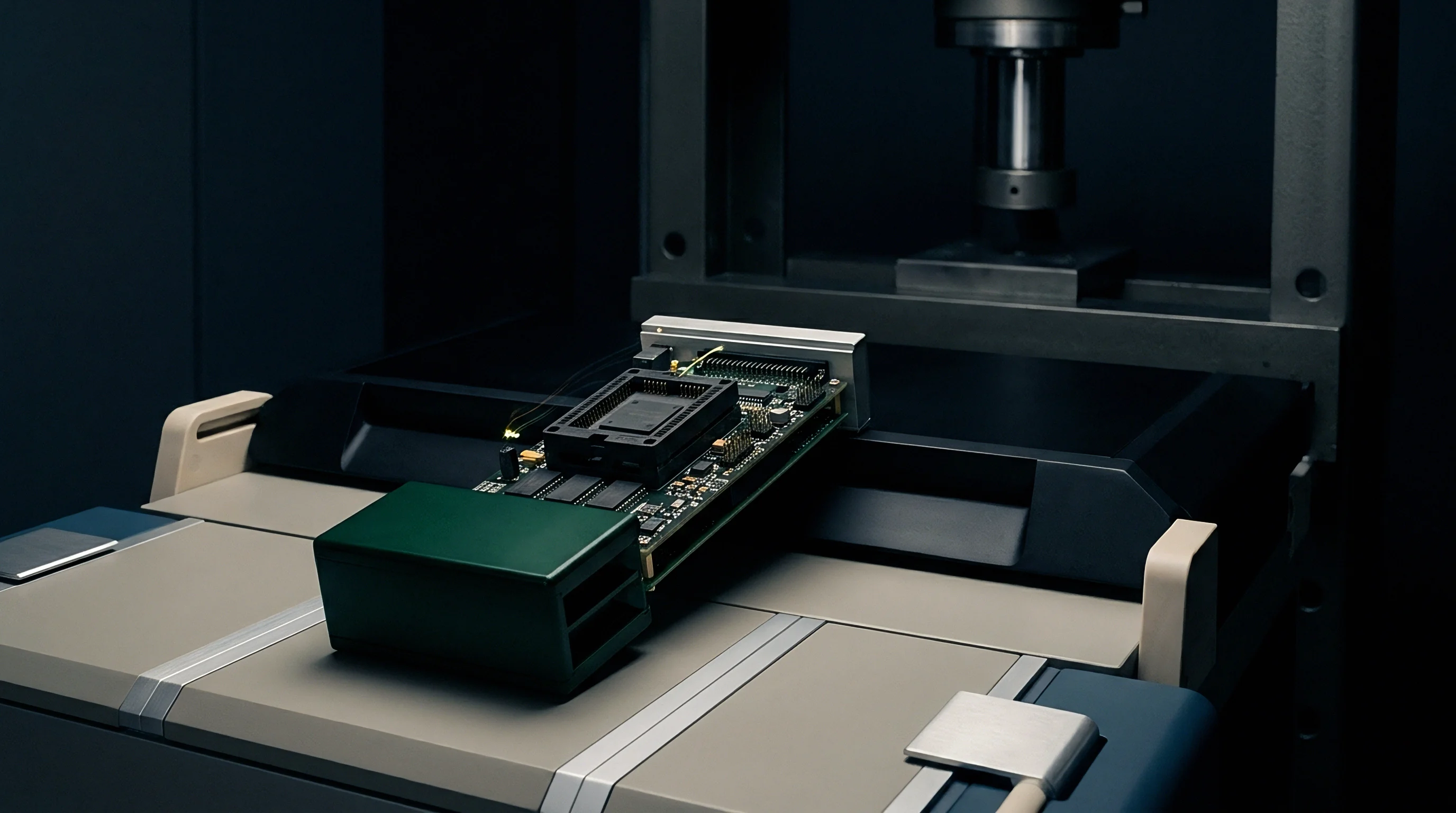
Distortion
Signal corruption across serial lines drives microcontroller software into edge-case recovery paths. Inducing controlled degradation requires hardware-level arbiters operating at the bit level. Microcontroller communication controllers react differently to physical signal shifts compared to logical protocol violations.
Automated hardware-in-the-loop setups alter differential signal amplitude, duty cycle timing, phase alignment, and rise time parameters while remaining synchronized to ongoing bus traffic.
Controller Area Network and Controller Area Network Flexible Data-Rate protocols rely on bit-stuffing rules to maintain clock synchronization across distributed nodes. An FPGA-driven fault injector counts transmitted bits in real time and suppresses bit-stuffing transitions by driving dominant logic levels over recessive bit slots. Driving six consecutive dominant bits forces every listening node on the bus to signal an active error frame.
The test system calculates the exact microsecond timestamp of bit insertion to test whether microcontroller software correctly enters bus-off state or corrupts internal memory queues.
Injecting a 350-millivolt differential voltage drop below standard transceiver threshold forces targeted bit sampling errors within individual frames.

Differential Voltage and Timing Deviation Setup
Precise manipulation of differential voltage levels exposes margins in internal analog comparator logic within microcontroller transceivers. Standard ISO 11898-2 specifies recessive differential voltage between minus five hundred and plus fifty millivolts, with dominant differential voltage between one and a half and three volts. Hardware injection boards alter these levels via programmable digital-to-analog converters driving high-speed line drivers.
Lowering the dominant differential voltage down to nine hundred millivolts simulates degraded physical bus lines, forcing targeted transceivers to read dominant bits as recessive.
Phase clock jitter injection degrades synchronous buses like Serial Peripheral Interface and Inter-Integrated Circuit interfaces. Injecting phase clock jitter involves delaying individual clock edges using programmable digital delay lines operating with picosecond resolution. Phase shift applied to the clock line relative to data setup and hold requirements exposes microcontroller register sampling errors.
The injection rig varies edge delays continuously across hundreds of test iterations to quantify exact timing limits before data corruption occurs.
Because mechanical relays chatter under rapid cycling, automated stress rigs manage fast signal transients with solid-state switches instead.
| Bus Interface Standard | Nominal Bus Voltage (V) | Injected Differential Offset Range | Injected Clock Skew Maximum | Target Error Response |
|---|---|---|---|---|
| CAN-FD (ISO 11898-2) | 2.0 to 3.0 (Diff) | -1.2 V to +0.8 V | ± 40 ns per bit bit-rate dependent | Stuff error, active error frame, bus-off |
| LIN (SAE J2602) | 12.0 (Single-Ended) | -3.5 V to +2.0 V relative to VBAT | ± 2.5 µs bit timing jitter | Header sync failure, checksum mismatch |
| I2C Fast-Mode Plus | 3.3 to 5.0 (Single-Ended) | 0 V to 1.8 V low-level noise injection | 120 ns clock hold stretch override | Bus freeze, clock stretch timeout, arbitration loss |
| SPI (4-Wire High Speed) | 1.8 to 3.3 (Single-Ended) | 0 V to 0.8 V ground rebound simulation | 15 ns setup time violation window | Data bit shift, register corruption, frame length error |
| 100BASE-T1 Ethernet | 1.0 (Peak-to-Peak Diff) | -400 mV to +300 mV amplitude shift | 1.2 ns phase jitter on PAM-3 clock | Symbol error, packet drop, link re-negotiation |

Sequential Fault Injection Rules
Controlled protocol verification demands running stress scripts in structured steps. Injecting randomized failures without deterministic baseline controls leads to non-reproducible software bugs. The test procedure forces isolated physical degradation first, followed by protocol-level bit manipulation, and concludes with bus contention flooding.
- Apply target power and establish baseline zero-error frame transmission across five thousand consecutive frames.
- Shift bus dominant voltage downward in increments of fifty millivolt steps until the target microcontroller registers an error counter increment.
- Trigger FPGA bit manipulation to corrupt the frame CRC field exactly on the forty-second bit position of the payload.
- Inject continuous dominant bit holding to force target microcontroller CAN controller into bus-off state.
- Monitor microcontroller recovery timing against standard software specification requirements.
- Restore nominal electrical levels and log total time elapsed prior to target node automatic bus re-integration.
Because transceivers lock when drives overlap, corrupting physical layer parameters without tracking internal microcontroller state registers leads to unclassifiable system hangs that obscure software protocol bugs.


Fixture
Hardware-in-the-loop stress testing relies on integrated test fixtures containing programmable power supplies, matrix routing boards, FPGA controller cards, and target execution controllers. High-density fixtures route hundreds of signal connections through standard mass-interconnect interfaces to simplify swap-outs between different target microcontrollers. Signals route through isolated trace layers on high-layer-count printed circuit boards designed specifically to maintain fifty-ohm single-ended and one-hundred-ohm differential impedance across all test paths.
Real-time execution engines command hardware injection boards through low-latency real-time Ethernet or PCI Express sub-networks. The host computer sends high-level fault profiles to an onboard FPGA, which handles nanosecond-accurate signal manipulation independently of host operating system timing jitter. Shielding sensitive analog feedback loops prevents switching transients generated by automated power supplies from contaminating low-voltage bus lines and corrupting test logs.
Adherence to ISO 26262 ASIL-D fault mitigation mandates physical injection proving that target software recovers from bus-off events within forty milliseconds.

How Do Physical Layer Switches Induce Transceiver Lockup?
Transient short circuits across differential pair buses create instantaneous voltage spikes on transceiver internal supply rails. When a solid-state switch short-circuits CAN High to twelve-volt battery lines, excess current flows backward into the transceiver driver circuit. Internal protection diodes clamp the voltage, but high current forces the driver substrate into latch-up.
Transceiver latch-up grounds the internal communication bus, preventing the target microcontroller from transmitting or receiving further communication until an external power reset cycle clears the fault.
FPGA logic units manage complex real-time fault scenarios by continuously monitoring bus line states via ultra-fast comparators. When detecting a specific frame identifier, the FPGA triggers inline switches within twenty nanoseconds. This speed enables modifying selected bits within a single frame payload while leaving preceding header bits and trailing acknowledge bits completely uncorrupted.
To prevent timing jitter from disrupting frame synchronization, high-precision hardware fixtures enforce deterministic execution down to single clock cycles of the FPGA system clock.
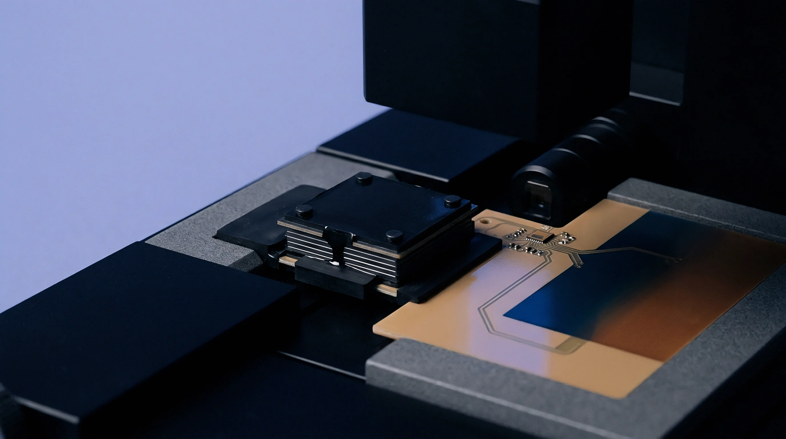
FPGA Core Integration and Edge Logic
Custom FPGA cores execute fault pattern state machines loaded over host control queues. The FPGA holds pattern tables defining exact bit locations, delay durations, and fault types. Using hardware-based state machines guarantees exact repetition of test sequences, allowing software engineers to step through microcontroller register states with an in-circuit debugger during fault events.
- Mass Interconnect Interface establishes high-density, low-wear electrical contact blocks rated for ten thousand mating cycles.
- FPGA Injection Card houses high-speed logic blocks running at four hundred megahertz for single-nanosecond bit slicing and signal manipulation.
- Programmable Power Rail Injector induces voltage drops down to zero point eight volts for microsecond intervals to test brownout behavior during bus activity.
- High-Bandwidth Matrix Board routes bus lines dynamically to switch topology configurations between star, linear, and stub networks under program control.
- Galvanic Isolation Barrier protects fixture control electronics from high-voltage transients induced during destructive bus stress tests.
Harness length variations introduced during fixture assembly are often treated as negligible in production, but in practice even minor deviations degrade high-speed differential bus stress profiles.

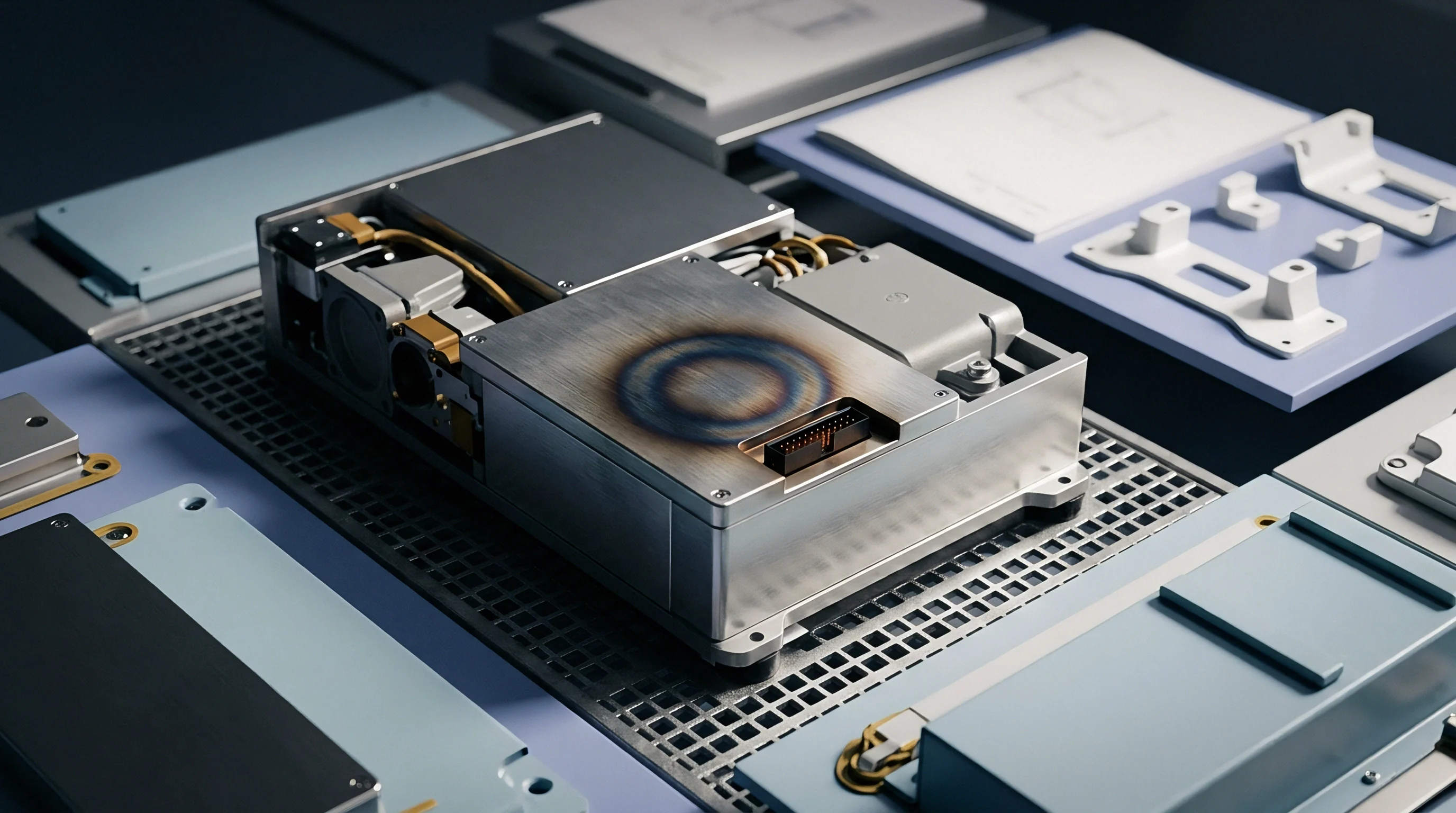
Audit
Quantifying test results requires systematic correlation between injected physical anomalies and microcontroller system reactions. Test logs collect high-resolution oscilloscope digital samples alongside target microcontroller internal software logs captured via high-speed trace interfaces like Serial Wire Debug or Nexus instrumentation pins. An automated test campaign executes tens of thousands of individual fault variations, generating gigabytes of trace data that demand automated parsing scripts to detect silent failures.
Silent failures occur when physical bus corruption fails to trigger an immediate hardware interrupt, allowing corrupted data to pass into application memory layers before detection. Automated audit frameworks cross-reference exact timestamps of injected bus errors against internal microcontroller software task execution timestamps. A time delta exceeding application control loop execution limits indicates unacceptable software recovery latency.
Automated log analysis engines catch silent data corruption by correlating hardware pin injection timestamps against internal software trace logs with nanosecond resolution.

Stress Execution Cycle Economics
Manual bus stress testing yields low test case density and poor reproducibility across complex silicon revisions. An engineer using manual bench tools executes approximately fifty distinct fault injection test cases per day. An automated hardware-in-the-loop bench executes over ten test cases per second, accumulating over eight hundred thousand test cases across a twenty-four-hour continuous execution run.
Evaluating financial allocations for automated test infrastructure involves comparing upfront non-recurring engineering costs against engineering labor required for manual validation. Developing custom FPGA injection IP, designing high-density routing fixtures, and scripting automated test suites requires significant capital commitment. This capital investment yields rapid paybacks across multi-year microcontroller software integration projects through dramatic reductions in manual regression testing time.
| Evaluation Metric | Manual Bench Testing Setup | Semi-Automated Rack Setup | Fully Automated HIL Bench Setup |
|---|---|---|---|
| Initial NRE Tooling Expense | 12,000 USD | 45,000 USD | 135,000 USD |
| Test Case Execution Speed | 0.001 Hz (50/day) | 0.2 Hz (720/hour) | 15.0 Hz (54,000/hour) |
| Fault Injection Timing Accuracy | ± 50 ms (Manual trigger) | ± 1 µs (Software trigger) | ± 2.5 ns (FPGA clock trigger) |
| Coverage across 10,000 Combinations | Under 1 percent per week | 15 percent per week | 100 percent in under 3 hours |
| Traceability to ISO 26262 Requirements | Manual log signing | Exported CSV logs | Automated database mapping to REQ-IDs |

Coverage Analysis for Edge Failure Modes
Mapping stress test cases to functional safety requirements ensures full audit compliance under automotive and industrial standards. System safety concepts define specific bus failure conditions that target microcontrollers must handle without entering unsafe operational modes. Stress test suites calculate code coverage metrics from internal microcontrollers while executing bus injection matrices to verify that error-handling routines execute in full under real hardware stress.
Simulating transient field faults through combined stress vectors, such as bus line short circuits paired with low target supply voltage, exposes silicon lockup states that pass isolated component tests.
Under Clause 8.4.2 of ISO 26262-10, hardware stress testing deliverables must contain deterministic, timestamped signal traces proving full software state recovery following induced bus physical layer failures.

Settlement
Transferring automated hardware-in-the-loop stress testing capabilities between engineering houses, turnkey solution suppliers, and manufacturing partners demands clear deliverable boundaries. Disputes over test bench performance usually stem from poorly defined software repository structures, missing calibration profiles, or ambiguous non-recurring engineering line items. A comprehensive design transfer package includes full hardware schematics, Gerber files, FPGA register maps, script source code, and calibration records covering every signal injection path.
Turnkey engineering contracts must explicitly assign ownership rights for custom FPGA fault injection cores and test script libraries. Third-party test houses frequently provide bench hardware built on proprietary software frameworks, creating long-term lock-in for ongoing regression testing. Securing complete Python source code and CAPL script files enables internal engineering teams to maintain, modify, and run test suites independently across future microcontroller silicon iterations.
Tagging code repositories and documenting hardware dependencies prevents test scripts from breaking when host control software or real-time operating systems are upgraded.
- Hardware Fabrication Package transfers altium schematics, board stackup definitions, Gerber X2 manufacturing files, and bill of materials with specific component manufacturer part numbers.
- FPGA Injection Core Source Code delivers VHDL or Verilog source files, synthesis constraints, bitstream build scripts, and internal register map documentation.
- Test Execution Suite Source provides Python, CAPL, or LabVIEW test scripts with full revision history, modular library files, and continuous integration pipeline hooks.
- Fixture Calibration Dossier contains trace impedance measurement reports, relay contact resistance baselines, and signal propagation delay maps for every channel.
- Acceptance Test Dossier defines standardized factory acceptance test procedures, baseline reference log files, and verification criteria for bench sign-off.
Defining clear maintenance scopes guarantees that suppliers update fault injection libraries when target microcontrollers transition to new silicon revisions with altered register maps. Equipment acceptance signed off without full FPGA IP transfer leaves the buyer dependent on the original vendor for every minor test profile modification over the product lifecycle.