Meaning
Electromagnetic energy generated by a device and propagated through space constitutes the unintended field measurement which governing bodies limit to prevent interference with nearby electronic systems. The phenomenon involves high frequency currents traveling through circuits that act as antennas, which then release signal power into the local environment. Compliance authorities mandate strict testing protocols to ensure that equipment operates within defined power density boundaries, preventing malfunctions in adjacent hardware or communication channels.
Designers manage these physical effects by balancing circuit layout, shielding, and filtering strategies. The measurement boundary occurs where the intentional wireless transmission ends and the non-functional energy transfer begins, defining the limit between a product function and a regulatory violation.
Frequency Calibration
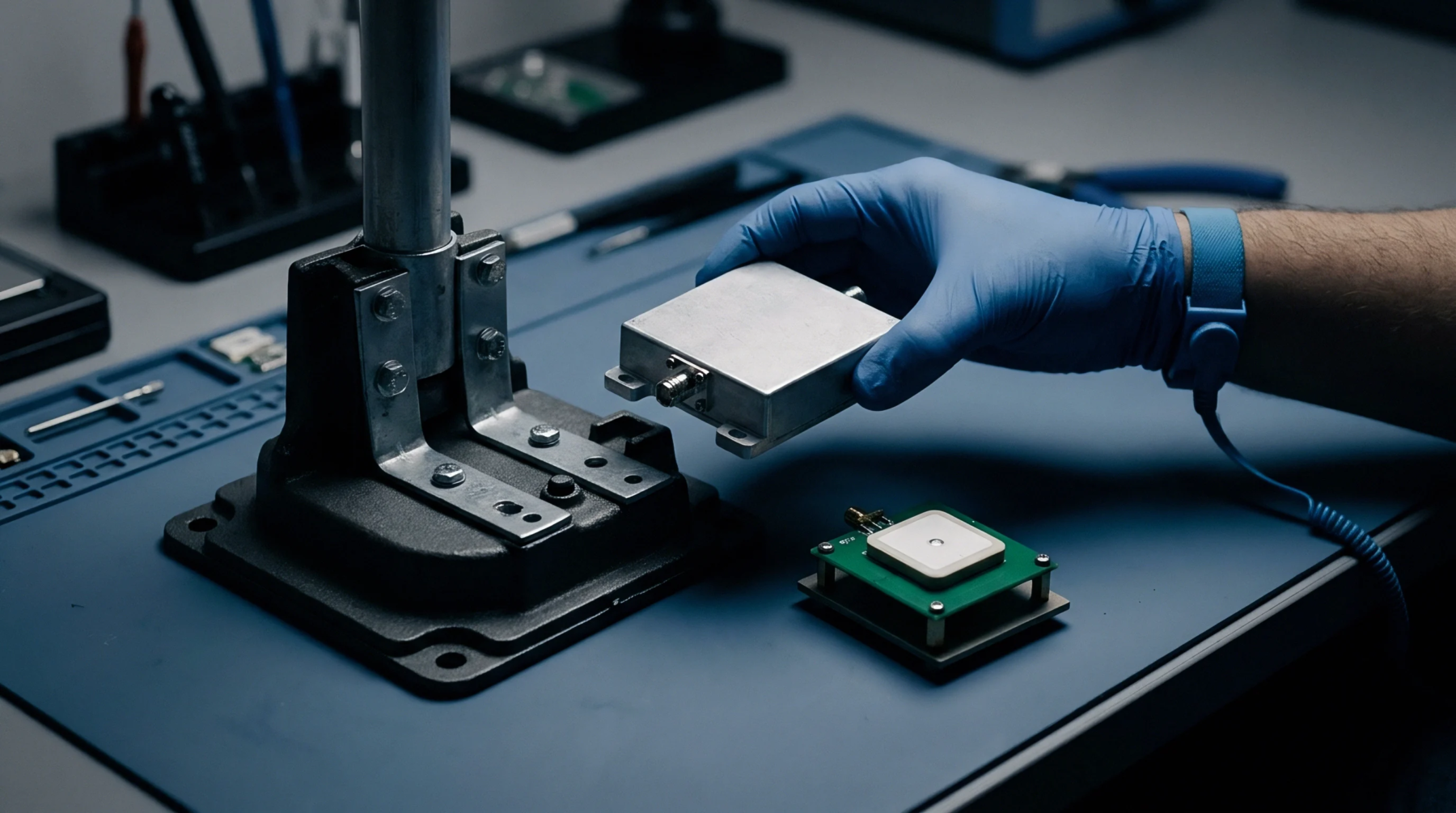
Evaluation protocols require placement of the device under test inside an anechoic chamber to isolate signals from ambient external noise. Engineers use calibrated receivers and specialized antennas to scan across a broad range of spectral bands to identify any peak power levels that exceed the allowable threshold defined by regional standards. This sequence begins at low frequencies where components might act as dipole antennas and continues up to gigahertz ranges where parasitic capacitance dictates field behavior.
Observations during this assessment phase reveal specific internal clock harmonics or supply switching frequencies that leak outside the protective chassis. Once the capture process concludes, the data provides a baseline for determining if the layout necessitates additional grounding paths or ferrite suppressors to mitigate signal leakage.
Circuit Interaction
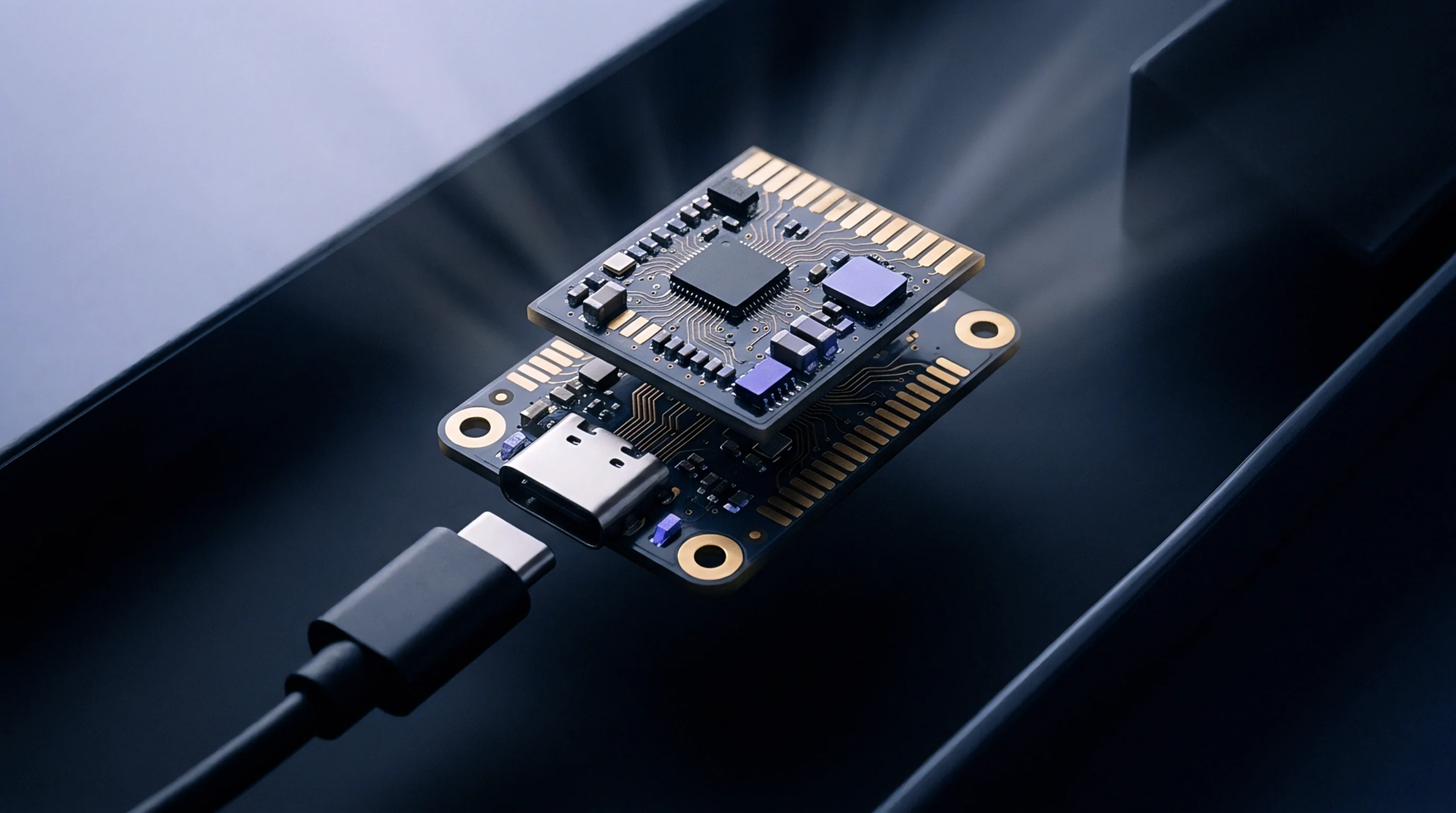
Physical geometry of the internal board assembly defines the efficiency at which an electronic module releases energy into the atmosphere. Conductive traces act as transmission lines that allow currents to escape if the return path provides too much impedance, forcing signals to seek alternative routes back to the ground plane. These paths often bridge the gap between digital processing units and external ports, effectively creating a loop that broadcasts high frequency noise.
Increasing the density of a board often requires tighter control over these return currents, as shorter spacing reduces the physical area of loops while minimizing the inductive coupling between adjacent traces. Shielding cans placed over sensitive processors prevent local fields from reaching board edges where they would otherwise couple to interface cables and extend the transmission surface area.
Compliance Verification
Certification documentation requires a summary of measurements that demonstrates how the assembly meets the hardware standard without exceeding safe levels under typical operating loads. Labs evaluate the total system rather than individual components to account for the way metal housings and external cabling modify the behavior of the final package. A device often passes component tests but fails at the assembly stage because the mechanical enclosure creates a resonance effect that amplifies specific signal harmonics.
Each handover document must state the precise configuration of cables and software states used during the test to guarantee that the results represent the actual product performance under field conditions. Future updates to the hardware require retesting because even minor layout adjustments affect the total field profile and shift the emission peaks. This physical property of electronic systems determines the ultimate viability of a design in complex environments.