Managing Modular Approval Compliance and Regulatory Re-Qualification Risks in Scale Hardware Production
Managing modular compliance requires maintaining strict reference trace layouts, securing firmware power tables, and contracting vendor liability for permissive changes.


Grant
Modular integration approvals rely on strict adherence to reference conditions set during Telecommunication Certification Body test suite executions. When a radio module receives a Full Modular Approval under Title 47 of the Code of Federal Regulations, Part 15.212, or equivalent Innovation, Science and Economic Development Canada RSS-Gen standards, the grant holder certifies that the device meets regulatory limits independent of a specific host chassis. The authorization rests on explicit hardware boundaries: an integrated RF shield, regulated power supply feeds, buffered data inputs, and a dedicated permanent or unique antenna connector.
Deviating from any single constraint invalidates the baseline filing and reclassifies the module as a Limited Modular Approval. Regulators reject unlisted elements.
Host integrators frequently misunderstand the boundary between modular authorization and host-level compliance. Incorporating a certified radio module does not exempt the end product from unintentional radiator testing under FCC Part 15 Subpart B or CISPR 32 standards. The host board itself introduces parasitic ground loops, switching noise from power converters, and clock harmonics that couple into the radio structure.
When host ground planes under the module trace keep-out area carry high-speed digital signals, radiated spurious emissions routinely breach class limits.
Radiated emissions margin drops by 4.2 dB when host ground planes under the module trace keep-out area are populated with high-speed digital lines.
Maintaining modular validity requires matching the host interface layout to the module manufacturer’s exact evaluation board specifications. Power supply rail ripple must remain strictly beneath specified limits, typically under 15 millivolts root-mean-square, to prevent phase noise degradation in the transmitter local oscillator. Co-location of multiple transmitters introduces further regulatory hurdles.
Placing a modular cellular transceiver within 20 centimeters of a Wi-Fi module on the same host PCB triggers mandatory Specific Absorption Rate evaluation and multi-transmitter intermodulation testing.
- Buffer Capacitance Compliance Integration designs maintain dedicated low-ESR decoupling capacitors within 2 millimeters of host power pins to prevent supply droop during transmit bursts.
- Keep-Out Layer Enforcement Multi-layer host PCBs clear all copper layers beneath the printed inverted-F antenna geometry across a minimum 15-millimeter perimeter.
- Trace Impedance Matching RF signal paths between module pads and external SMA connectors follow controlled microstrip dimensions calibrated to 50 ohms nominal impedance.
- Co-Location Assessment Dual-radio host systems measure combined maximum permissible exposure figures before committing to final enclosure plastics tooling.
Under 47 CFR Section 15.212(a)(1)(ii), the inclusion of buffered data inputs shifts legal responsibility for timing jitter and over-modulation from the host board integrator directly back to the module original equipment manufacturer.
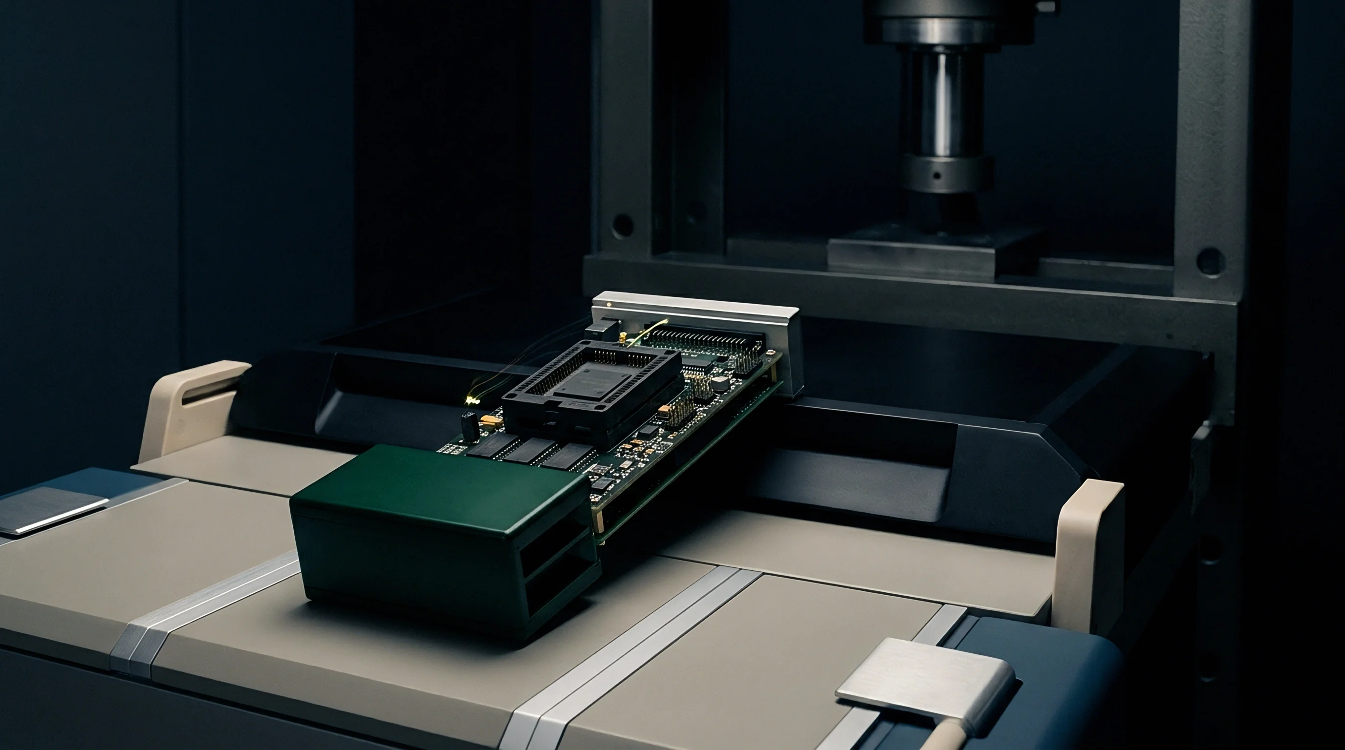
Shield
RF containment covers welded or soldered directly over baseband circuitry establish the boundary between transmitter certification and host board noise contamination. A modular approval requires that all radio frequency components, baseband processors, and synthesizer loops possess independent shielding. Bends in RF microstrip traces created without ground-plane void relief cause localized impedance shifts that reflect harmonic energy into adjacent digital circuits.
The physical shield prevents external electromagnetic fields generated by host power supplies from modulating the radio local oscillator.
Altering the physical shield structure on a certified module automatically voids the modular grant. Host integration teams attempting to shrink vertical envelope dimensions by removing the soldered shield cover trigger a mandatory complete transmitter re-authorization. The presence of the metal shield affects the thermal dissipation paths and dielectric loading of the underlying circuit traces.
Radiated emissions margins measured without the factory shield installed invariably fail radiated spurious emission limits at fundamental harmonics.
| Layout Parameter | Reference Value | Tolerance Limit | Non-Compliance Consequence |
|---|---|---|---|
| Microstrip Trace Width | 0.50 mm | +/- 0.02 mm | Impedance shift exceeding 5 ohms, driving antenna mismatch loss |
| Substrate Dielectric (Er) | 4.20 | +/- 0.15 | Shift in coplanar waveguide propagation velocity and phase delay |
| Ground Via Pitch | 1.25 mm | +/- 0.10 mm | Spurious RF leakage at upper harmonic frequencies above 5 GHz |
| Coplanar Ground Gap | 0.25 mm | +/- 0.015 mm | Radiated spurious emissions breach Class B statutory limits |
| Data measured across 50-ohm grounded coplanar waveguide test coupons on FR4 substrate. | |||
Trace routing from the module RF pin to an external antenna pad represents a critical point of regulatory vulnerability. Sourcing teams changing the PCB stack-up or prepreg material supplier alter the dielectric constant of the RF path. Impedance mismatches at the module boundary reflect power back into the power amplifier, causing high-order intermodulation products.
Traces alter radiated field patterns. Coupling shifts peak harmonics.
Bends in RF microstrip traces created without ground-plane void relief cause localized impedance shifts that reflect harmonic energy into adjacent digital circuits.
Deviating from the certified microstrip trace geometry without filing a permissive change forces a complete host-level intentional radiator re-certification that incurs lab fees exceeding thirty thousand dollars and delays production shipping by up to twelve weeks.

Patch
Regulatory locks within system firmware define power output boundaries across regional spectrum allocations. Modern wireless modules employ software-defined radio controls where operating frequencies, maximum output power, and channel bandwidths are governed by non-volatile configuration memory. FCC KDB 594280 D01 guidance enforces strict software security requirements to ensure that third parties cannot alter RF parameters beyond certified limits.
Attenuators reduce peak power. Firmware seals the power profile.
Integrating a module into a host product requires absolute alignment between the host operating system driver and the certified module firmware binaries. Modifying a driver parameter to increase throughput can inadvertently disable adaptive frequency hopping or dynamic frequency selection protocols mandated for UNII band operation. Power tables dictate country codes.
Silicon revisions alter driver timing.
- Download the exact binary firmware release hash specified in the module manufacturer regulatory submission dossier.
- Flash the non-volatile memory region containing regional radio configuration tables via encrypted factory programming tools.
- Verify that host driver software calls enforce power table locks across all operating temperature extremes.
- Execute automated radio test scripts to confirm dynamic frequency selection thresholds respond within regulatory millisecond limits.
- Lock production board JTAG access interfaces to prevent post-assembly modification of non-volatile radio parameters.
Software change management protocols in scale manufacturing facilities must treat radio driver code with the same control level applied to physical hardware revisions. Updating a host Linux kernel driver can alter how the host board manages power state transitions in the radio chipset. If a power state transition causes the module to briefly exceed its maximum authorized output power during bootloader execution, the host unit breaches market compliance rules.
Module vendors frequently assert that firmware updates delivered via closed binary blobs automatically preserve regulatory status, omitting the reality that modified driver interface calls can alter transmit duty cycles beyond tested limits.

Shift
Component end-of-life notices and silicon die shrinks alter the internal parasitic behavior of radio frequency front-end circuits. When a semiconductor manufacturer executes a process node transition for an RF power amplifier or baseband chip, the physical characteristics of the silicon change. Although the functional specifications remain identical on the datasheet, high-frequency harmonic generation and thermal drift profiles diverge from the original qualification sample.
Sourcing changes alter noise floors. Layout shifts breach grant bounds.
Passive component substitutions during production scaling represent a major source of compliance decay. Replacing a surface-mount inductor in an RF matching network with an alternative part number that matches nominal inductance often fails compliance due to differences in self-resonant frequency and quality factor. Inductance drives harmonic peaking.
Certificates follow exact component part numbers. Factories sign false conformance claims.
Pursuant to IPC-1735 material declaration protocols, an unannounced substitution of an RF matching network inductor voids host-level compliance certificates and breaches master supply agreements.
- Passive Component Tolerances Swapping C0G dielectric ceramic capacitors for X7R variants introduces voltage coefficient capacitance shifts that detune RF output filters.
- Crystal Oscillator Phase Noise Alternative crystal vendors exhibiting higher phase noise increase transmitter adjacent channel power leakage beyond regulatory limits.
- Printed Antenna Materials Changing PCB laminate suppliers alters substrate loss tangent values, damping antenna resonance and altering total radiated power figures.
- Enclosure Coating Conductance Metallic pigment variations in enclosure plastics shielding paints alter near-field coupling and alter spurious harmonic radiation.
Managing component changes requires structured engineering change order regimes connected to regulatory impact assessments. Tooling transfers incur lab delays. Spurious emissions breach mask edges.
The engineering practice evaluates every proposed bill-of-materials modification against the original laboratory test reports to determine if RF performance boundaries remain uncompromised.
A change in crystal oscillator supplier requires spectrum analyzer verification of fundamental frequency stability across the entire operating temperature envelope before production packaging begins.


Class
Regulatory bodies define exact boundaries between administrative documentation updates and mandatory laboratory re-testing. In the FCC framework, modifications to certified intentional radiators fall into Class I or Class II Permissive Changes. A Class I Permissive Change addresses modifications that do not degrade degradation profiles, including minor layout adjustments or equivalent passive substitutions, requiring no formal filing with the agency.
A Class II Permissive Change applies when hardware alterations increase radiated emissions or change thermal characteristics while remaining within statutory limits, requiring official filing and TCB review.

When Does a Passives Swap Force Class II Compliance?
Substituting passive components in an RF path triggers Class II Permissive Change procedures whenever the measured emission levels increase compared to the original certification test data. If an alternative component supplier increases peak radiated spurious emissions by more than 0.5 dB, even if the total emission level remains below the legal limit, the regulatory framework requires a Class II filing. Replacing an internal antenna with a higher-gain model or altering trace routing dimensions beyond documented tolerances similarly demands formal re-qualification.
| Hardware Modification Type | Filing Classification | Mandatory Testing Scope | Regulatory Submission |
|---|---|---|---|
| Equivalent Passive RF Filter Swap | Class I Permissive Change | In-house spot check of conducted output power | Internal compliance dossier update |
| Enclosure Plastic Density Alteration | Class I Permissive Change | Radiated spurious emissions verification | Internal compliance dossier update |
| Antenna Gain Increase under 2 dBi | Class II Permissive Change | Full radiated emissions and SAR evaluation | TCB filing and public database update |
| Shield Cover Geometry Change | Class II Permissive Change | Radiated spurious emissions and power density | TCB filing and public database update |
| Baseband Silicon Node Shrink | New Equipment Authorization | Complete Part 15 transmitter test suite | New FCC ID grant application |
Establishing robust qualification dossiers demands meticulous file maintenance. Sourcing groups must maintain technical documentation that links every physical production iteration back to its corresponding regulatory submission file.
- Original Test Reports Raw frequency sweeps, plot printouts, and calibration logs generated during primary TCB certification testing.
- Permissive Change Justification Written engineering analysis detailing why specific bill-of-materials adjustments meet Class I or Class II criteria.
- Antenna Pattern Measurement Three-dimensional radiation pattern plots verifying gain limits across all operating bands.
- Co-Location SAR Evaluations Mathematical modeling and laboratory probe data proving safety compliance for multi-radio host layouts.
Whether regulatory agencies will eventually require mandatory continuous-monitoring telemetry for software-controlled power tables in multi-radio host environments remains an open policy debate.

Lien
Commercial liability for non-compliant hardware rests on the contractual allocation of regulatory ownership between module supplier and host integrator. When a non-compliant transmitter reaches market, regulatory enforcement agencies hold the final host manufacturer accountable for market withdrawals and administrative fines. Standard module supply agreements frequently limit vendor liability to the simple replacement cost of defective hardware, leaving host integrators fully exposed to millions of dollars in recall expenses and lost commercial distribution access.
Sourcing agreements must establish explicit compliance escrow mechanisms and design custody terms. Obtaining full Gerber files, firmware source repositories, and raw laboratory test files ensures that host integrators can execute compliance filings independently if the module supplier dissolves operations or refuses to support necessary permissive change applications. The landed cost of a radio module must incorporate potential re-qualification contingencies across the full volume production lifecycle.
Retaining original test laboratory raw data files inside secure compliance escrows protects host integrators against supplier insolvency during market audits.
| Re-qualification Event Scope | Laboratory Engineering Cost | Schedule Delay Duration | Production Line Risk Level |
|---|---|---|---|
| Class I Spot Check Verification | $3,500 – $6,000 | 1 – 2 Weeks | Low: Production continues during testing |
| Class II Permissive Change Filing | $15,000 – $28,000 | 4 – 6 Weeks | Medium: Shipments paused pending TCB review |
| Full New Equipment Authorization | $45,000 – $85,000 | 10 – 14 Weeks | High: Complete factory halt and tooling freeze |
| Multi-Radio SAR Safety Re-evaluation | $12,000 – $22,000 | 3 – 5 Weeks | Medium: Enclosure redesign risks |
| Summary reflecting average commercial testing laboratory rates and TCB filing fee structures. | |||
Engineering scope agreements specify precise responsibilities for regulatory re-testing costs driven by component obsolescence. If a module vendor changes an RF front-end component to address their own supply chain shortages, the master services agreement mandates that the vendor covers all associated host-level Class II permissive change testing costs. Defining these terms before issuing volume purchase orders prevents costly disputes when component markets force mid-lifecycle manufacturing changes.
Establishing clear contractual custody over test reports, firmware signing keys, and Gerber source files ensures that host manufacturing lines continue operating without regulatory disruption when component supply chains force rapid layout adaptations.