Evaluating Permissive Change Compliance Paths for Potted RF Transmitter Modules
Adding potting compound to an unpotted RF module demands Class II permissive change re-testing if dielectric loading increases radiated spurious emissions.

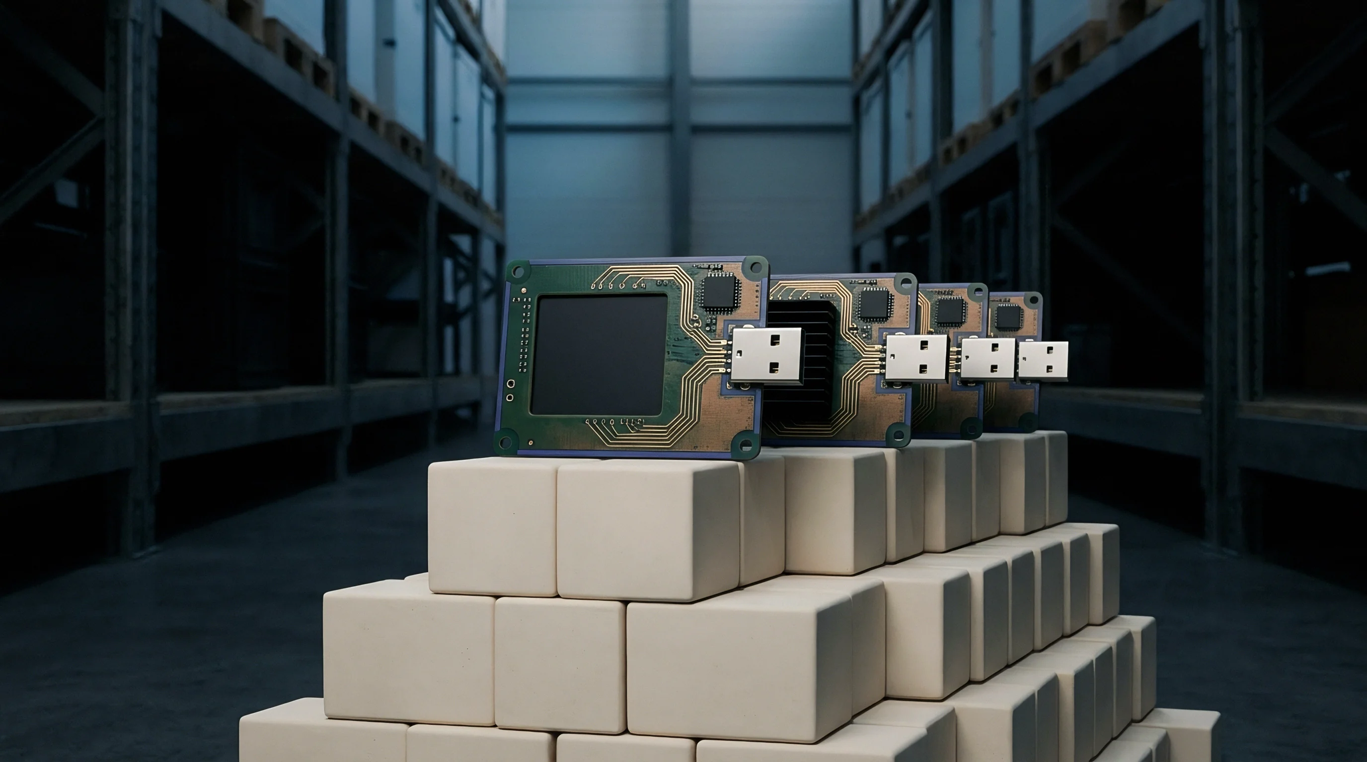
Resin
Pouring liquid encapsulant over bare surface-mount radio assemblies immediately reshapes local electromagnetic fields. When a potting compound displaces air across a circuit board, the relative permittivity around microstrip traces, surface-mount inductors, and printed antenna elements jumps from roughly 1.0 to somewhere between 2.8 and 5.5. That dielectric loading adds parasitic capacitance across RF signal paths, drops the characteristic impedance of 50-ohm transmission lines down to 38 or 42 ohms, and slows wave propagation across the substrate.
Unshielded matching networks detune on contact, dragging the fundamental resonant frequency lower and degrading input return loss.
The extent of this drift depends heavily on the compound chemistry and its curing mechanics. Two-part epoxies, polyurethanes, silicones, and fluoropolymer resins show widely varying dielectric constants and loss tangents across industrial temperature ranges. A high loss tangent introduces direct attenuation into the RF path, converting transmitter power into heat inside the resin matrix.
That thermal penalty quickly compounds when power amplifiers sit trapped in thick polyurethane blocks without dedicated conduction paths to external heat sinks.
A 3.5 dB increase in second-harmonic radiated emissions occurs when two-part polyurethane covering an unshielded power amplifier exceeds a dielectric constant of 3.8 at 2.4 GHz.
In high-density potted modules, harmonic peaks trace back to localized dielectric shifts near power amplifier output networks. Solid fill creates unintended capacitive coupling between closely spaced traces. Adding a metal shield can resolve this entirely: by enclosing the RF section, the shield isolates the near-field reactive region from the potting compound and prevents dielectric loading on critical matching parts.
Encapsulating an unshielded module, by contrast, leaves every trace geometry, passive component, and crystal oscillator open to mechanical strain and electrical detuning.

Dielectric Loading and Circuit Detuning
Air has a relative permittivity near 1.0, whereas liquid potting compounds typically measure between 2.8 and 5.5. This difference directly alters the distributed capacitance of microstrip runs on standard FR-4 or high-frequency polyimide substrates. Because the characteristic impedance of a microstrip line drops with the square root of the effective dielectric constant, a line designed for 50 ohms in air can fall to 40 ohms under solid polyurethane, introducing impedance mismatches at component interfaces and driving up the voltage standing wave ratio.
Printed trace antennas and surface-mount chip antennas take the worst hit from direct resin contact. An antenna’s reactive near-field extends roughly one-sixth of a wavelength outward from the radiating element. Flooding that volume with high-permittivity dielectric material stores electric field energy, which pulls the resonant frequency down and narrows usable bandwidth.
Matching networks calibrated for free air can no longer balance the detuned antenna, reflecting substantial power back into the final amplifier stage.

Thermal Shrinkage and Stress Induction
Curing cycles bring volumetric shrinkage that applies real mechanical force to surface-mount passives. Epoxies often contract by 1 to 3 percent during cross-linking, placing ceramic chip capacitors, ferrite inductors, and quartz crystal cans under continuous compression. Microphonic behavior and piezoelectric strain within ceramic layers then show up as spurious phase noise and carrier jitter.
Mismatched coefficients of thermal expansion among the resin, PCB substrate, and component solder joints create steady shear forces across thermal cycles. As temperatures swing, crystal oscillators can drift past their allocated channel tolerances. Compressional stress on inductors also shifts core permeability, nudging inductance values in active bandpass filters off-target and degrading out-of-band rejection.

Spurious Generation and Parasitic Paths
Filling board air gaps with solid compound creates stray capacitive pathways between adjacent traces. Because higher relative permittivity increases mutual capacitance across parallel runs, crosstalk between digital lines and sensitive RF nodes rises. Noise from switching regulators can bleed straight into synthesizer supply rails, generating unwanted sideband spurs.
Power amplifier stages also run into non-linear behavior as dielectric loading pulls output matching networks off-spec. The resulting standing wave ratios reflect energy back into active transistor junctions, generating harmonic distortion products. Harmonic energy that original filter stages once suppressed can then slip past detuned filter elements, creating radiated emission spikes that threaten regulatory limits.
Physical failure modes arising from potting compound selection manifest across electrical, mechanical, and thermal performance vectors:
- Impedance Mismatch microstrip lines tuned for 50 ohms shift down to 38 ohms under high-permittivity fill, raising voltage standing wave ratios.
- Harmonic Radiated Peaks stray capacitance alters output filtering network poles, allowing second and third harmonics to breach Class B limits.
- Frequency Pulling mechanical strain on unshielded crystal oscillators shifts fundamental carrier frequencies beyond allocated channel bandwidth limits.
- Antenna Efficiency Degradation embedded trace antennas experience severe near-field detuning, dropping total radiated power by up to 6 dB.
| Material Family | Dielectric Constant (1 GHz) | Loss Tangent (1 GHz) | Volumetric Shrinkage (%) | Primary RF Degradation Vector |
|---|---|---|---|---|
| 4.0 – 5.5 | 0.020 – 0.035 | 1.5 – 3.0 | Severe antenna detuning and crystal mechanical stress | |
| 3.2 – 4.2 | 0.015 – 0.025 | 0.5 – 1.5 | Moderate impedance shift and thermal dissipation limits | |
| 2.7 – 3.1 | 0.001 – 0.005 | < 0.2 | Low dielectric loading; minor near-field detuning | |
| 2.1 – 2.4 | 0.0005 – 0.0015 | 0.8 – 1.2 | Minimal electrical drift; high material material unit cost |
Selecting an unapproved liquid compound without chamber pre-scans triggers full filing rejections and forces complete re-engineering of the module enclosure.
Classification
Regulatory agencies enforce rigid procedural rules for any physical changes made to certified wireless hardware. Under FCC rules in 47 CFR § 2.1043, modifications to intentional radiators are categorized into permissive change tiers depending on how they affect output power, occupied bandwidth, and spurious emissions. Adding potting resin to an unpotted module certified under modular approval rules alters its physical construction, requiring thorough validation against baseline grant data.
Choosing the correct filing route hinges on precise conducted and radiated measurements. A Class I Permissive Change applies when modifications cause zero degradation in RF parameters, generate no new spurious emissions, and keep power strictly within original tolerances. If the resin causes minor spurious emission increases while staying below regulatory ceilings, the change falls under Class II.
Should fundamental parameters shift out of specification or operational bands change, the modification requires a full equipment authorization under a new identifier.
Under 47 CFR § 2.1043, any modification altering the outer enclosure dimensions or internal RF field distribution of an approved module without permissive change documentation renders the equipment authorization void.
Under the European Radio Equipment Directive (2014/53/EU), the administrative concept of permissive changes does not exist in the FCC sense. Instead, manufacturers conduct internal risk assessments to verify continued compliance with Article 3.2 spectrum efficiency requirements. Potting an unencapsulated module obligates the manufacturer to re-test against relevant Harmonised Standards, such as ETSI EN 300 328 for 2.4 GHz equipment or ETSI EN 300 220 for sub-GHz radios.
Once testing confirms compliance, the manufacturer updates the Technical Documentation File and issues a revised EU Declaration of Conformity; Notified Body involvement is not required unless the original type examination certificate scope explicitly demands it.

Class I Permissive Change Boundaries
Modifications that introduce no degradation and keep all transmitter metrics within original test margins qualify for simple administrative documentation updates. For example, injecting potting compound under a sealed metal shield where RF components remain isolated from direct material contact is typically handled as a Class I change. Because fields stay confined within the shield cavity, trace impedance, output power, and spurious harmonics align with initial certification data.
Confirming Class I eligibility requires comparative bench testing against original baseline reports. Conducted power figures must match within standard measurement uncertainty (usually 0.5 dB), and radiated pre-scans must show no new harmonic peaks or elevated spurs. The manufacturer logs these comparison plots in internal compliance records without needing to submit a formal filing to a Telecommunications Certification Body.

Class II Permissive Change Triggers
Any measurable increase in radiated emissions or changes to RF exposure models require formal laboratory reports and TCB review. Pouring potting compound directly onto bare traces, unshielded power amplifiers, or printed antennas alters the physical build and RF spatial distribution. Even if emissions stay well beneath statutory limits, any measurable increase in radiated field strength triggers a Class II filing.
Specific Absorption Rate or Maximum Permissible Exposure calculations also need updating if the compound alters separation distances between antennas and user tissue, or shifts near-field boundary conditions. A Class II filing requires an accredited lab report, updated internal and external photos, a formal cover letter, and review by a TCB before updated units can be shipped.

European Radio Equipment Directive Assessment
For products sold in the European Union, manufacturers must document their risk assessments under standard conformity assessment procedures. Because encapsulation changes physical construction, the device must be evaluated against the essential requirements of RED Article 3.1b (EMC) and Article 3.2 (radio spectrum). The technical rationale must specifically address unwanted emissions in the spurious domain under ETSI EN 300 328 clause 4.3.2.9.
If re-testing verifies compliance with published harmonised standards, the economic operator updates the Technical Documentation File retained under Annex II. Involving an EU Notified Body is generally optional unless the original certificate restricted encapsulation changes. That said, failing to keep comparative test records in the technical file invalidates the CE marking, leaving the manufacturer vulnerable to market surveillance actions.
Evaluating an encapsulated module modification requires verifying specific physical and electrical conditions against regulatory rules:
- Fundamental Power Verification conducted output power measurements stay within a strict 0.5 dB tolerance window compared to original grant records.
- Out-of-Band Emission Audits radiated spurious emissions remain below established regulatory limits with at least a 3 dB margin reserve.
- Shielding Configuration Integrity the original metallic shield remains intact without mechanical modification during compound application.
- Antenna Pattern Uniformity total radiated power and gain profiles show no degradation across operational frequency channels.
| Regulatory Authority | Filing Classification | Technical Trigger Conditions | Required Documentation Submittal | Administrative Review Time |
|---|---|---|---|---|
| Class I Permissive (C1PC) | Zero RF parameter degradation; power within 0.5 dB; zero spurious increase | Internal test data retained in quality management file | Zero days (Instantaneous internal release) | |
| Class II Permissive (C2PC) | Measurable spurious emission increase below limit; RF exposure recalculation | TCB submittal: Test report, Form 731, photos, cover letter | 7 to 14 business days | |
| New Equipment Authorization | Circuit modifications; shift in operational bands; fundamental power shift | Full certification dossier submittal under new FCC ID | 14 to 21 business days | |
| Class 4 Permissive (C4PC) | Modifications to certified modular approval without altering RF circuits | Radio Equipment List update via Canadian TCB | 10 to 15 business days | |
| Internal TDF Revision | Re-testing confirms compliance with ETSI EN 300 328 / EN 301 489 | Updated Technical Documentation File and revised EU DoC | Zero days (Self-declaration completion) | |
| Type Attribution Notification | Minor enclosure changes; solid filling without RF layout alteration | Notification letter and spot-check test plots to Registered Certification Body | 10 to 20 business days |
Section 15.21 of the FCC rules stipulates clear warning notices in product documentation specifying that unauthorized module potting voids the operator authority to use the device.


Verification
Anechoic chambers isolate the electromagnetic shifts introduced by solid potting compounds. To build a solid permissive change case, engineers must systematically measure radiated spurious emissions, occupied bandwidth, peak power, and radiation patterns. Test setups must mount the potted module inside standardized fixtures to isolate board-level drift from any resonance contributed by the host enclosure.
Radiated testing requires full 360-degree turntable sweeps across both antenna polarizations in 3-meter or 10-meter semi-anechoic chambers. Direct conducted RF power measurements frequently become impossible once micro-coaxial test ports or trace pick-off points are submerged in cured resin. When ports are inaccessible, engineers must rely on calibrated radiated methods, factoring in antenna gains and cable losses to calculate Equivalent Isotropically Radiated Power.
When potting compound directly touches an unshielded printed antenna, radiated harmonic emissions consistently increase while antenna gain drops.
During anechoic testing, second-harmonic emissions surged by 4.2 dB after potting an unshielded 2.4 GHz transmitter. A disciplined test plan gathers baseline data on unpotted units, then repeats the identical sweep on potted samples prepared with the exact production resin and cure schedule. Automated spectrum analyzer routines sweep from 9 kHz through the tenth harmonic of the fundamental frequency to catch any spurious energy born from dielectric loading on active amplifier stages.

Radiated Spurious Emission Scans
Turntable sweeps in 3-meter semi-anechoic chambers quickly reveal harmonic peaks caused by potting mass around RF power amplifiers. Radiated fields from bare traces interact with the resin layer, introducing secondary refraction effects. Test software steps the turntable through 15-degree azimuth increments, recording peak and average responses across horizontal and vertical measurement antenna polarizations.
Harmonic checks must verify that out-of-band emissions comply with general limits in FCC Part 15.209 or ETSI EN 300 328 clause 4.3.2.10. Special care is needed near ISM band edges, like the 2400 MHz to 2483.5 MHz boundary. Dielectric detuning that widens the occupied bandwidth causes spectral energy to bleed over the edges, potentially violating restricted band limits under FCC Part 15.205.

Near-Field SAR and Exposure Evaluation
Changing the physical thickness between an embedded antenna and the outer casing alters spatial absorption in biological tissue. Specific Absorption Rate testing quantifies RF deposition in tissue-simulating liquids according to IEC/IEEE 62209-1528 standards. Because potting changes the complex permittivity profile in the near field, peak 1g or 10g spatial SAR values can shift.
If potting alters outer enclosure dimensions, the minimum separation distance between radiating elements and user skin shifts with it. A reduction in effective separation can spike localized SAR, voiding an existing modular SAR exemption. Re-evaluations under FCC KDB 447498 D01 or ISED RSS-102 demand full area and zoom scans to establish revised spatial-average SAR metrics for Class II submittals.
Occupied Bandwidth and Spectral Mask Audits
High-resolution spectrum analyzer sweeps capture channel power distributions to verify band-edge compliance. Either conducted or radiated setups measure 20 dB bandwidth and 99 percent occupied bandwidth profiles under full modulation. Setting resolution bandwidth filters strictly to regulatory requirements ~ such as 100 kHz for sub-GHz bands or 1 MHz for microwave allocations ~ maintains a consistent noise floor.
Transmitters using complex digital modulations, like OFDM or QAM, often experience sideband regrowth when dielectric loading pushes power amplifiers into non-linear operation. Automated test scripts overlay post-encapsulation masks onto baseline grant traces. Any spread beyond authorized channel boundaries requires retuning matching circuits or re-evaluating the resin formulation.
A structured laboratory execution protocol validates compliance parameters sequentially:
- Mount the unencapsulated transmitter on the dielectric turntable at 1.5 meters height inside the 3-meter semi-anechoic chamber.
- Record baseline conducted power, occupied bandwidth, and radiated spurious emissions up to the tenth harmonic.
- Apply the designated encapsulation compound using production-line dispensing equipment and cure according to manufacturer thermal profiles.
- Repeat full 360-degree turntable scans across all orthogonal planes to identify worst-case electric field emissions.
- Compare post-encapsulation emission levels against baseline records to establish whether changes remain within Class I thresholds.
A pre-scan conducted on a single prototype unit saves weeks of wasted chamber booking fees before submitting formal documentation to certification bodies.

Dossier
Regulatory filings depend on clear technical documentation demonstrating that modified radio hardware remains fully compliant. Preparing a Class II Permissive Change package for a Telecommunications Certification Body requires methodical assembly of physical, electrical, and procedural records. This dossier serves as an auditable technical trail proving the potted assembly meets every applicable rule clause.
Certification bodies evaluate packages under formal accreditation guidelines, checking test setups, instrument calibration dates, and sample configurations against standard procedures. Photo documentation should be assembled prior to compound application. A complete submission contains administrative forms, an engineering explanation of the potting process, high-resolution internal photos, and comparative test reports signed by accredited lab personnel.
Class II permissive change filings require direct side-by-side photographic evidence proving component placement remains identical before and after liquid compound dispensing.
The documentation must specify whether the potted unit is certified as a standalone module or only as part of a specific host assembly. If the modular grant restricts physical alterations or potting over bare traces, the applicant must provide engineering proof that shielding integrity remains uncompromised. Updates to host OEM manuals must clearly outline potting limits, approved resin types, and required enclosure clearances.

Test Report Architecture and Exhibits
TCBs review calibrated measurement plots alongside detailed setup notes to validate the requested filing path. A lab report prepared for a Class II filing covers equipment configurations, antenna gain profiles, test software versions, and chamber environmental conditions. Test plots must clearly identify fundamental carriers, harmonic markers, limit lines, and applied transducer correction factors.
Summary tables lay out field strength values directly against regulatory limits and include calculated margins. Signatures from test engineers and lab quality managers confirm the measurements were taken in ISO/IEC 17025 accredited facilities. Including raw log files and spectrum analyzer captures ensures a smoother, faster administrative review.
Photographic Evidence and Schematics
High-resolution photographs must document board layouts before and after compound dispensing. Internal photos should show the bare PCB, component placement, solder joints, and shield attachment points, while post-potting photos need to demonstrate fill depth, surface leveling, and edge sealing.
Schematic diagrams submitted with the package confirm that no active or passive component values were altered during potting. The applicant includes an explicit declaration that trace routing, ground planes, and amplifier matching networks remain untouched. If schematics were altered during the potting rollout, the change falls outside permissive change rules and must be filed under a new FCC ID.

Host Integration Guidance Updates
Modular approval grants pass definite legal obligations downstream to host integrators. When a manufacturer certifies a potted module option, the integration manual must specify approved potting compounds, cure cycles, and mechanical clearance requirements.
These integration guides instruct host builders on thermal management, shielding requirements, and trace routing for external antennas. If the design uses an embedded printed antenna that reacts to surrounding materials, the guide must detail plastic wall thicknesses and keep-out distances. Failing to update host documentation leaves downstream integrators exposed during market surveillance audits.
A complete Class II Permissive Change application package requires specific technical exhibits:
- Permissive Change Cover Letter formal written narrative detailing exact physical modifications, material compositions, and electrical reasoning supporting the filing path.
- Accredited Laboratory Test Report full measurement dataset including antenna plots, radiated spurious emission tables, and calibrated instrument serial records.
- Comparative Component Schematics engineering drawings confirming zero active or passive component substitutions occurred during the potting process.
- Internal Module Photographs unencapsulated and fully potted module photographs showing compound coverage, layer thickness, and shield boundary conditions.
Even minor chemical variations in potting resins can alter radiated radio frequency performance.


Ledger
Commercial launch schedules hinge on choosing compliance routes that balance review times against lab costs. Planning regulatory paths for encapsulated wireless products requires a clear view of direct testing fees, lab lead times, and international filing prerequisites. Misclassifying a permissive change can trigger unplanned re-testing, stranding inventory while market windows narrow.
Financial modeling balances internal validation costs against outside chamber fees and agency surcharges. Structuring global filing schedules around accredited lab availability prevents launch delays. Relying on Class I internal documentation minimizes outside filing fees, but requires sufficient in-house test capability to verify zero RF parameter drift.
A Class II filing incurs accredited lab and TCB review fees, but remains far cheaper than running full original certifications across multiple international target markets.
Filing a Class II permissive change costs less than one-third of a new modular certification while preserving existing regulatory grant IDs across global target markets.
International markets introduce separate filing dependencies. An FCC Class II grant does not grant automatic approval elsewhere. Selling in Canada requires a parallel ISED Class 4 Permissive Change filing.
European markets call for updating internal Technical Documentation Files and issuing revised Declarations of Conformity. In Japan (MIC/Giteki) and South Korea (KC), physical modifications can trigger specific notifications or spot-check tests, adding local agent and translation costs to the project ledger.
Laboratory and Certification Cost Modeling
Direct compliance costs cover chamber time, engineering reports, and certification body administrative fees. Booking an accredited 3-meter semi-anechoic chamber generally costs between 1,500 USD and 3,000 USD per day. A typical Class II test suite for radiated spurious emissions and occupied bandwidth consumes two to three chamber days, including setup.
TCB review fees for FCC C2PC filings run between 1,200 USD and 2,500 USD per application, with additional charges for expedited handling or joint ISED filings. By comparison, a completely new equipment authorization requires full transmitter characterization across all channels, easily pushing laboratory fees past 15,000 USD per country. Taking the permissive change route protects the initial grant investment and narrows testing to the altered parameters.
Filing Timelines and Queue Mechanics
Project delays multiply quickly if a certification body issues technical inquiries or requests re-tests. Laboratory booking queues represent the most volatile variable in the schedule, with accredited facilities booked out two to six weeks depending on seasonal volume. Reserving chamber time early keeps milestones on track.
Administrative reviews add more calendar time once testing concludes. TCB review of a Class II filing takes seven to fourteen business days after receiving the final report. If reviewers raise questions about dielectric parameters or SAR modeling, responses can add several weeks.
In jurisdictions requiring local representative filings ~ such as ANATEL in Brazil or SRRC in China ~ administrative lead times can easily stretch by four to eight weeks.
| Compliance Route Tiers | Accredited Test Chamber Cost (USD) | Certification Body Administrative Fee (USD) | Laboratory Lead Time (Weeks) | Agency Review Lead Time (Weeks) | Total Execution Window (Weeks) |
|---|---|---|---|---|---|
| 500 – 1,500 (Internal pre-scan) | 0 (Internal retention) | 0.5 – 1 | 0 | 0.5 – 1 | |
| 3,000 – 7,500 (Targeted re-test) | 1,200 – 2,500 | 2 – 4 | 1.5 – 3 | 3.5 – 7 | |
| 12,000 – 22,000 (Full test suite) | 3,500 – 6,000 | 4 – 8 | 3 – 5 | 7 – 13 | |
| 2,000 – 5,000 (Harmonised spot-check) | 0 (Self-declaration) | 1 – 3 | 0 | 1 – 3 | |
| 2,500 – 6,000 (Local RCB spot-check) | 1,500 – 3,000 | 3 – 6 | 2 – 4 | 5 – 10 |
Whether emerging high-frequency millimeter-wave modules can ever undergo post-grant potting without requiring entirely new hardware certifications remains uncertain across international regulatory working groups.