Resolving Host Integration Emissions and Radiated Spurious Discrepancies across Multi-Radio Embedded Architectures
Resolving host-integrated radiated spurious discrepancies requires systematic decoupling, strict ground continuity, and precise co-location testing.

Spurs
High-density layouts place wireless modules right next to switching regulators and high-speed memory buses. Inside a cramped host enclosure, the RF environment bears little resemblance to a vendor’s clean evaluation setup. Unintended electromagnetic coupling produces host-integration emissions and unexpected radiated spurious peaks, causing designs to fail compliance testing even when built around a certified module.
Resolving those spikes means tracking down board-level coupling paths, parasitic radiators, and clock harmonic injection points.
Host integration failures typically show up on chamber scans as sharp spectral spikes or broad noise pedestals. Broadband digital noise from processors, PMICs, and display interfaces couples directly into front-end traces and antenna feeds, which then re-radiate that interference through the antenna. Conversely, strong RF fundamentals can rectify inside host ESD protection diodes, generating secondary spurious tones that leak past chassis seams and cabling.
Trace inductance radiates, common-mode noise eats up chamber margin, and dropping local shielding patches onto the board rarely solves the root issue.

Mechanisms of Parasitic Radiation in Host PCB Design
Current loops on a PCB act as magnetic dipoles. High-frequency signals on microstrip traces induce return currents in the ground plane directly beneath them. When ground slots, thermal reliefs, or split planes interrupt that return path, current must detour around the gap.
This expanded loop area boosts radiated magnetic fields in proportion to the loop size and the square of the frequency. Above 1 GHz, millimeter-scale discontinuities in the plane turn into slot antennas, completely bypassing local decoupling.
Routing traces across PCB layers introduces via transitions that break the return path. When a signal via changes reference planes without an adjacent stitching via, return current must find a high-impedance route through a distant ground via or inter-plane capacitance. That high-impedance loop converts differential noise into common-mode voltage, driving current onto host structures such as metal frames, heatsinks, and external cabling.
Unshielded cables then behave like quarter-wave monopole antennas, turning internal common-mode current into radiated emissions that easily exceed Class B limits.
Radiated spurious emissions from high-speed digital lines frequently surpass transmitter harmonics when microstrip traces bridge discontinuous ground planes.
Ground plane impedance frequently drives host-induced spurs. Fast digital switching currents passing through parasitic via and trace inductance trigger high-frequency ground bounce. This shifts local ground potential beneath the radio module, modulating its reference ground relative to the main board.
That potential difference drives common-mode noise into RF matching networks and antenna feeds, while stray capacitance between shield cans and nearby traces creates a secondary path that dumps high-order digital harmonics straight into the transmitter output.

High-Speed Bus Switch-Noise and Clock Harmonic Injection
Digital buses such as PCIe, USB 3.2, and MIPI CSI generate broad harmonic trains that land directly inside common wireless bands. A 100 MHz PCIe reference clock, for example, produces odd and even harmonics extending past 6 GHz. Running host traces parallel to module interfaces allows capacitive and inductive crosstalk to dump clock harmonics straight into the RF front end.
Receiver LNAs saturate, while power amplifiers mix host clock harmonics with the carrier frequency to radiate intermodulation spurs.
Switch-mode supplies operating between 1 MHz and 3 MHz produce high-energy transients with sub-nanosecond rise times. These sharp edges ring against parasitic inductance and capacitance in the power distribution network, generating high-frequency noise from 100 MHz to 800 MHz. Unshielded switching inductors spill magnetic fields into nearby microstrips, while rail noise leaks into LNA supply lines, modulating the carrier and creating sideband spurs that violate spectral mask limits.
Display interfaces frequently cause spurious emissions due to their long trace lengths and high data rates. MIPI D-PHY signals running at 1.5 Gbps per lane radiate heavily at fundamental clock frequencies and their harmonics. Impedance discontinuities along differential pairs convert differential data signals into common-mode currents, which couple into nearby structural elements and excite the host enclosure, turning internal digital switching into radiated emissions that mask weak RF signals and trigger chamber failures.
Module vendors usually blame customer host emissions on poor ground plane design, shifting the responsibility for structural shielding back onto the integrator.


Pin
The connector interface is the primary boundary where host noise passes the radio module shield. Multi-pin headers, LGAs, and board-to-board connectors introduce parasitic inductances and open field paths that compromise RF isolation. Noise coupling across interface pins corrupts transmitter spectral purity and degrades receiver sensitivity through near-field crosstalk.
Resolving these spurious issues requires tight control over power rail impedance, pinout geometry, ground stitching density, and shield continuity.
Pin mapping along module edges directly dictates EMC performance. Interleaving ground pins between high-speed data lines isolates return paths and lowers mutual inductive coupling. If power lines run adjacent to noisy digital signals without ground separation, voltage transients leak straight into the radio supply domain.
Forcing multiple return currents through a single ground pin leads to common-impedance coupling, pulling digital noise directly into the radio ground reference. High-density layouts rely on dedicated ground fencing around sensitive analog and RF traces.

Power Rail Decoupling and Ground Loop Impedance
Switch-mode supplies push high-frequency current ripple directly into transceiver power pins. Effective decoupling requires low-ESR capacitors placed right at the pins. A single 100 nF capacitor loses effectiveness above 50 MHz due to internal parasitic inductance.
Broadband decoupling relies on parallel combinations of 100 pF, 10 nF, and 1 uF capacitors, using smaller package footprints to handle higher frequencies, with ferrite beads adding extra attenuation at the upper boundary.
Ground loop impedance between the host motherboard and radio daughtercard generates common-mode noise. Connecting ground planes through sparse pins forces high-frequency return currents through elevated RF impedance, creating localized voltage drops across connector pins that drive common-mode noise onto external cables and metal housings. Continuous ground connections around the module perimeter clear out these impedance bottlenecks and prevent common-mode voltage buildup.
Power distribution network impedance must remain low across a wide frequency band. On multi-layer host boards, high-frequency supply ripple correlates directly with sideband spur amplitudes during transmit sweeps. Adding local ceramic capacitors with self-resonant frequencies matched to the spur frequencies suppresses peak rail ripple, while low-parasitic surface-mount parts keep ground impedance low enough to stop switching transients from reaching the RF front end.
Shielding Can Aperture Leakage and Cable Coupling
Enclosure seams and connector slots turn into effective slot antennas as their physical length approaches a quarter-wavelength. Metal shield cans attenuate radiated energy only when ground connections remain continuous. Thermal cutouts or mounting clip slots in shield walls leak high-frequency magnetic fields; at 5 GHz, a 15 mm slot behaves as a half-wavelength antenna, letting internal RF escape directly into host cavities.
Internal coax running from module u.FL connectors to host antennas represents another common path for spurious emissions. Low-quality shielding braid leaks energy along its entire length due to poor optical coverage, while common-mode currents on the outer braid radiate freely. Routing coaxial cables across switching regulators or memory buses picks up near-field noise and dumps it straight into the antenna port.
Cable orientation relative to host traces largely dictates how much noise couples across.
Physical failure modes in host assemblies frequently cause radiated emission spikes during regulatory testing:
- Discontinuous Shielding Seams caused by wide ground pad spacing let high-frequency magnetic fields leak past internal shielding.
- High-Impedance Power Vias without nearby decoupling capacitors pass switching transients right into sensitive RF supply rails.
- Unterminated Cable Braids carrying common-mode current act as quarter-wave monopole antennas, boosting digital noise across regulatory bands.
- Floating Metallic Heatsinks near high-frequency components pick up near-field energy and re-radiate spurious harmonics.
- Reference Ground Plane Splits crossed by high-speed differential traces force return currents into wide loops, converting differential noise into common-mode emissions.
Apertures in shield covers must remain significantly smaller than the shortest operational wavelength. Conductive gaskets, spring fingers, and tight solder spacing maintain electrical continuity across joints. Containment degrades rapidly if surface oxidation or mechanical warping creates gaps, as high frequencies readily leak through small openings.
Adding conductive tape or grounding screws around shield perimeters restores containment.
Routing high-speed data traces perpendicular to reference ground splits reduces magnetic coupling into nearby transceiver circuits.


Chamber
Anechoic test facilities measure radiated emissions by rotating the device through 360 degrees on a turntable while scanning the measurement antenna between 1 and 4 meters. Discrepancies between standalone module reports and host integration scans occur frequently ~ a radio module that cleared standalone testing easily can fail by over 10 dB once mounted inside a host enclosure. Resolving that gap requires auditing chamber geometry, turntable setup, antenna factor calibration, cable routing, and background noise floors.
Measurement uncertainty stems from several physical factors. Semi-anechoic chambers use ground-plane reflection with wall absorbers, whereas fully anechoic chambers line every surface with RF absorber. Site-to-site differences in reflections, antenna positioning, and quiet zone performance produce variations between labs.
Minor setup details ~ table materials, power cord runs, auxiliary gear placement ~ shift radiated patterns enough to create gaps between pre-scans and final qualification sweeps.
What Causes Chamber Discrepancies across Host Enclosures?
Standalone module certificates rest on evaluation boards tested in free space. Host integration places the module inside dense enclosures near metal frames, multi-layer PCBs, batteries, and display panels. These surrounding elements shift antenna matching, detune resonant frequencies, and distort radiation patterns.
Reflected power from impedance mismatches drives the final amplifier into non-linear behavior, generating new spurious emissions.
Enclosure materials govern internal reflections. Metal housings trap RF fields until they escape through seams, gaps, or plastic windows. Plastic enclosures offer minimal shielding, letting PCB trace radiation pass directly into the chamber.
Structural dimensions can also resonate at specific harmonic frequencies, forming cavity resonators that amplify local spurs. Grounding internal metal structures to the main PCB plane shifts these cavity resonances away from active transmit bands.
FCC Part 15 Class B radiated limits mandate electric field strength below 54 dBµV/m at 3 meters for frequencies exceeding 960 MHz.
Cable positioning remains a major source of measurement variance. Unshielded power cables act as antennas for internal common-mode noise. Although standards define cable length and bundling, subtle changes in cable orientation can shift measured radiation substantially.
Adding ferrite cores to auxiliary cables dampens common-mode currents so the chamber reads true host emissions rather than cable harness radiation.
Standardized Test Protocols and Measurement Uncertainty
Compliance testing relies on calibrated biconical, log-periodic, and horn antennas to cover sweeps from 30 MHz up to the 10th harmonic of the highest fundamental. Resolution bandwidth settings under standards like ANSI C63.4 and CISPR 16 define analyzer filter shapes. Peak detectors speed up initial pre-scans, but final compliance requires quasi-peak or average detectors, which register lower readings on periodic noise.
Scans run in both vertical and horizontal antenna polarizations to capture full electric field vectors while max-hold algorithms log peak emissions during turntable rotation. Near-field probing with magnetic loop antennas pinpoints noisy PCB regions before committing to full chamber runs ~ frequently uncovering radiated emissions higher than conducted predictions suggested. Matching near-field hotspots with far-field chamber peaks isolates the exact traces or components driving regulatory failures.
Systematic chamber diagnostics isolate host radiated spurious failures through a structured sequence:
- Execute Baseline Ambient Noise Sweeps in the chamber with the host powered down to confirm background noise stays at least 6 dB below limits.
- Perform Conducted Antenna Port Measurements via coaxial connection to a spectrum analyzer to check transmitter spectral purity and harmonic levels.
- Scan Host Power Off State Emissions with the host board fully energized but the radio disabled to isolate processor and power supply noise.
- Conduct Radiated Sweeps with Continuous Carrier Transmit forcing maximum output power across low, mid, and high channels.
- Map Surface Radiated Hotspots using E-field and H-field probes across the PCB to spot trace geometries driving peak emissions.
- Apply Targeted Ferrite and Shielding Modifications to high-emission nodes while monitoring real-time changes on the analyzer.
- Execute Final Calibrated Radiated Certification Sweeps across full 360-degree rotations and 1-to-4-meter antenna heights in both polarizations.
Quiet zone validation determines measurement repeatability across test sites. Reflection errors in semi-anechoic facilities introduce field intensity variations up to 4 dB. Antenna factor drift, cable loss changes, and receiver attenuator non-linearities expand that margin further.
Factoring a measurement uncertainty budget of ±4.1 dB into pre-scan targets prevents false confidence before formal submission.
| Regulatory Standard | Jurisdiction | Frequency Range | Detector Type | Spurious Emission Limit | Measurement Distance |
|---|---|---|---|---|---|
| FCC Part 15.209 / 15.247 | United States | 30 MHz ~ 88 MHz | Quasi-Peak | 40.0 dBµV/m | 3 meters |
| FCC Part 15.209 / 15.247 | United States | 88 MHz ~ 216 MHz | Quasi-Peak | 43.5 dBµV/m | 3 meters |
| FCC Part 15.209 / 15.247 | United States | 216 MHz ~ 960 MHz | Quasi-Peak | 46.0 dBµV/m | 3 meters |
| FCC Part 15.209 / 15.247 | United States | Above 960 MHz | Average / Peak | 54.0 dBµV/m / 74.0 dBµV/m | 3 meters |
| ETSI EN 300 328 (Wideband) | European Union | 30 MHz ~ 1 GHz | Effective Radiated Power | -36 dBm (approx 60 dBµV/m) | 3 meters |
| ETSI EN 300 328 (Wideband) | European Union | 1 GHz ~ 12.75 GHz | Effective Radiated Power | -30 dBm (approx 66 dBµV/m) | 3 meters |
| SRRC Type Approval Rules | China | 30 MHz ~ 1 GHz | Quasi-Peak / Peak | -36 dBm (Operating Band) | 3 meters |
| Giteki Ordinance No. 37 | Japan | 30 MHz ~ 26 GHz | Peak / Average | -26 dBm to -80 dBm band specific | 3 meters |
Engineers continue to evaluate whether AI-driven near-field scanners can accurately predict far-field compliance failures before host assemblies reach an anechoic chamber.

Coexistence
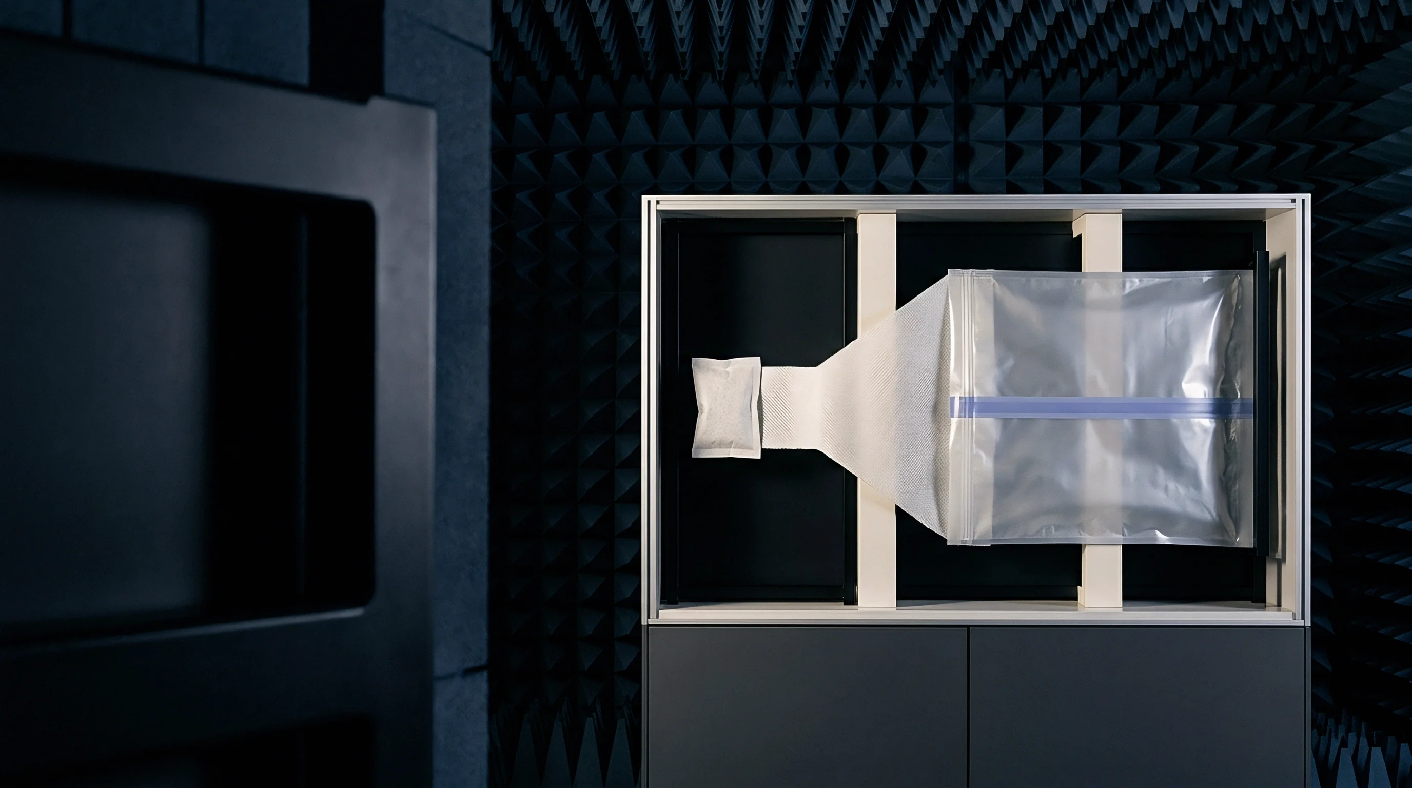
Running cellular, Wi-Fi, and Bluetooth transceivers at the same time creates complex RF mixing scenarios inside tight enclosures. Strong fundamental signals interact across non-linear components to produce intermodulation products, meaning radiated spurious failures often appear only during concurrent transmission. Fixing co-location issues requires auditing receiver front-end isolation, passive intermodulation sources, active mixing paths, and transmit filtering.
Intermodulation products landing in active receive bands or restricted spectrum cause both receiver desensitization and compliance failures. Third-order products are particularly troublesome because they fall close to active transmit channels. Fifth- and higher-order products have lower amplitude, but high transmit powers can still push them over strict spurious limits.
Dynamic frequency selection scenarios need thorough testing.

Intermodulation Product Generation in Dual Radios
Non-linear junctions generate intermodulation distortion when two transmitters operate simultaneously. Diodes and transistors in power amplifiers, LNAs, RF switches, and protection circuits go non-linear when driven by strong RF signals. If a 2.4 GHz Wi-Fi signal couples into an active LTE transmit path, the LTE power amplifier mixes the two signals, producing sum and difference frequencies that radiate out through the antenna system.
ETSI EN 301 489-17 Clause 7.1 specifies antenna port isolation requirements to prevent passive intermodulation in multi-radio host housings.
Passive intermodulation (PIM) happens when non-active components sit in strong electromagnetic fields. Oxidized metal joints, cold solder connections, loose fasteners, and ferromagnetic materials produce non-linear responses that radiate directly from structural frames. Tests on harmonic mixing between co-located Wi-Fi and Bluetooth radios confirm that passive mechanical joints act as secondary radiating sources during high-power multi-radio sweeps.
Antenna isolation sets the limit on cross-transmitter coupling. Placing 2.4 GHz and 5 GHz Wi-Fi antennas close together without spatial or polarization diversity yields isolation below 15 dB, allowing fundamental power from one transmitter to flood adjacent front ends. While integrated bandpass filters attenuate out-of-band harmonics, they cannot block intermodulation frequencies that fall directly inside their passband.

Co-Located Radiated Spurious Calculation Methods
Spectrum modeling calculates where sum and difference intermodulation products will fall. For transmitters at f1 and f2, third-order products land at 2f1 – f2, 2f2 – f1, 2f1 + f2, and 2f2 + f1. Modeling these product frequencies across active channel combinations highlights the exact spectrum blocks that require close scrutiny in the chamber.
Dual-tone intermodulation products follow standard combinations:
f_IM3 = |2 f1 ± f2| or |2 f2 ± f1|
f_IM5 = |3 f1 ± 2 f2| or |3 f2 ± 2 f1|
When calculated intermodulation products fall inside restricted bands defined by FCC Part 15.205 or ETSI EN 300 328, allowable limits drop sharply, placing strict isolation requirements on host layout.
| Transmitter 1 (f1) | Transmitter 2 (f2) | Calculated Order | Intermodulation Formula | Spurious Frequency | Regulatory Impact Zone |
|---|---|---|---|---|---|
| LTE Band 4 (1710 MHz) | Wi-Fi 2.4 GHz (2412 MHz) | 2nd Order (Diff) | f2 ~ f1 | 702 MHz | Cellular Downlink Band |
| LTE Band 4 (1710 MHz) | Wi-Fi 2.4 GHz (2412 MHz) | 3rd Order | 2 f1 ~ f2 | 1008 MHz | GPS / Aviation Band |
| Wi-Fi 2.4 GHz (2437 MHz) | Bluetooth (2480 MHz) | 3rd Order | 2 f1 ~ f2 | 2394 MHz | FCC Restricted Band 2390 MHz |
| Wi-Fi 5 GHz (5180 MHz) | Wi-Fi 2.4 GHz (2412 MHz) | 2nd Order (Diff) | f1 ~ f2 | 2768 MHz | Industrial Radiolocation |
| Wi-Fi 5 GHz (5805 MHz) | LTE Band 13 (777 MHz) | 3rd Order | f1 ~ 2 f2 | 4251 MHz | Altimeter Band Hazard |
Firmware can manage simultaneous transmission to suppress intermodulation. Time-division multiplexing prevents high-risk radios from transmitting in overlapping windows, while dynamic power reduction lowers output power during concurrent operation to keep intermodulation products below compliance thresholds.
FCC KDB Publication 996369 D04 Clause 2.2 requires host integrators running simultaneous transmitters to perform radiated verification across all active combinations ~ voiding self-declaration if intermodulation products breach compliance limits.


Grant
Modular filings specify exact operational conditions host integrators must meet to maintain compliance. Dropping a pre-certified module into a host device does not automatically transfer the approval to the finished product. Regulatory bodies such as the FCC, ISED, and European notified bodies enforce clear boundaries between modular authorization and final certification.
If host integration induces spurious emissions or alters antenna setup, the manufacturer must update the filings.
Modular approvals come as either full or limited grants. A full modular grant requires built-in RF shielding, onboard power regulation, a permanent or unique antenna connector, and standalone test results. Limited approvals apply when a module lacks one of these features, passing testing obligations to the host integrator.
Reviewing grant conditions early prevents regulatory holds and market distribution blocks.

Permissive Change Thresholds for Integrated Antennas
Replacing a certified trace antenna with an internal patch alters both radiation pattern and peak gain. FCC rules permit swapping antennas of the same type if gain is equal to or lower than the original grant. Using a different antenna type or higher gain requires mandatory re-evaluation; unauthorized changes invalidate the grant.
Permissive change rules dictate how modifications are filed. Under FCC guidelines, Class I Permissive Changes cover minor updates that do not degrade spurious emissions or RF parameters, requiring only internal records. Class II Permissive Changes (C2PC) apply when changes increase radiated emissions or modify RF exposure while staying under legal limits.
A C2PC requires accredited lab test data and TCB approval before product shipment.
Antenna gain modifications exceeding 2 dBi require formal Class II Permissive Change filings to maintain modular authorization validity.
ISED Canada uses a similar system spanning Class I to Class IV Permissive Changes, with Class IV specifically addressing co-located simultaneous transmitters not covered under the original filing. European CE RED rules do not use permissive change classifications; instead, host manufacturers must complete a risk assessment and update the Declaration of Conformity under Article 3.2.

Host Authorization Dossiers and Markings
End-product labeling provides physical evidence of compliance for customs and surveillance authorities. Hosts containing certified modules must display external markings showing the module’s unique regulatory IDs. Electronic labeling is acceptable on internal screens if user documentation clearly explains how to navigate to the compliance menu.
Maintaining technical documentation for each host integration variant requires pulling together supplier grants, host radiated test reports, co-location matrices, and updated labeling proofs for local agents to submit to regional bodies.
A decision checklist guides compliance categorization for host integration modifications:
- Antenna Gain Verification ~ Confirm replacement antenna gain stays below the maximum allowed in the modular grant.
- Antenna Type Matching ~ Verify the replacement antenna shares the same construction, polarization, and radiation characteristics as the certified reference.
- Separation Distance Evaluation ~ Measure the distance to human bodies to check if portable RF exposure rules apply instead of mobile limits.
- Co-Location Matrix Audit ~ Check if additional active transmitters sit within 20 cm of the radio module.
- Enclosure Shielding Assessment ~ Determine whether metallic housing elements detune the antenna or radiate secondary digital spurious noise.
- Filing Authorization Strategy ~ Decide whether changes qualify for a Class I internal file or require a formal Class II Permissive Change.
Integration technical files require validation before shipping. Incomplete dossiers weaken regulatory standing during market surveillance audits, whereas detailed documentation provides traceable proof of ongoing compliance across global markets.
Misclassifying host enclosure modifications can trigger customs holds, recall orders, and retroactive revocation of compliance certificates in regulated markets.

Budget
Qualification costs add up quickly across test runs, sample prep, and regional filings. Catching host emission failures late in laboratory testing causes expensive project delays, requiring extra chamber time, engineering redesign, and updated documentation. Keeping market access budgets intact requires planning test campaigns, sample counts, local representative fees, and filings strategically.
Lab rates vary by region and regulatory framework. Semi-anechoic chambers run 200 USD to 450 USD per hour, with full-day bookings running 2,500 USD to 5,000 USD. Pre-scan troubleshooting in lower-cost engineering chambers helps identify radiated spurious failures early, before committing to expensive formal certification sweeps.
Laboratory Fee Schedules and Retest Cost Mechanics
Accredited labs charge full daily chamber rates regardless of whether a device passes. Failing a radiated spurious sweep on day one of a three-day run halts testing, forcing the host back to the bench for PCB tweaks, shielding changes, or firmware power reductions. Lab rebooking queues often slip schedules by 3 to 6 weeks while original chamber reservation fees stay fully billable.
International market access adds administrative and agency costs. Jurisdictions such as China (SRRC), Japan (Giteki), Korea (KC), and Brazil (ANATEL) require specialized test protocols, local sample shipping, in-country representatives, and translation services. Tracking timelines across five international regulatory bodies helps sequence submittals efficiently and avoid redundant test fees.
| Regulatory Filing | Target Region | Required Test Samples | Average Lead Time | Direct Chamber Fees | Administrative Filing Fees |
|---|---|---|---|---|---|
| FCC Part 15 C/E (C2PC) | United States | 1 Conducted, 1 Radiated | 2 ~ 3 Weeks | $3,500 ~ $6,000 | $1,200 ~ $2,500 (TCB) |
| CE RED Assessment | European Union | 2 Radiated Final Units | 3 ~ 4 Weeks | $4,500 ~ $8,500 | $1,500 ~ $3,000 (Notified Body) |
| SRRC Type Approval | China | 2 Radiated, 1 Firmware Host | 5 ~ 8 Weeks | $7,000 ~ $12,000 | $2,000 ~ $4,000 (In-Country Agent) |
| Giteki Certification | Japan | 1 Conducted, 1 Radiated | 3 ~ 5 Weeks | $4,000 ~ $7,500 | $1,800 ~ $3,200 (RCB Fee) |
| KC Radio Mark | South Korea | 2 Complete Host Units | 4 ~ 6 Weeks | $5,000 ~ $9,000 | $2,200 ~ $4,500 (RRA Local Agency) |
| ANATEL Approval | Brazil | 2 Calibrated Test Samples | 6 ~ 10 Weeks | $6,500 ~ $11,000 | $3,000 ~ $5,500 (OCD Certification) |
Sequencing regulatory submittals keeps overall capital outlay under control. Running initial pre-scans at lower-cost local labs verifies radiated spurious performance before committing to expensive international filings. Parallel submission tracks shorten launch lead times, keeping product release schedules on target.
Aligning regional submittals reduces qualification costs while maintaining market availability across target countries.