Radio Frequency Interconnect Loss Driven by Substrate Dielectric Degradation Mechanisms
Substrate moisture absorption increases dielectric loss tangent, raising RF interconnect insertion loss and reducing long-term wireless link margins.
Trace
High-frequency signal transmission across printed circuit boards depends directly on the physical dielectric surrounding copper conductors. In microstrip, stripline, and grounded coplanar waveguide architectures, electromagnetic fields propagate not only through the metallic trace itself, but also through the bulk substrate material and the adjacent soldermask. High frequencies concentrate current.
Conductor loss dominates at lower radio frequencies, yet dielectric absorption scales linearly with frequency, dominating total interconnect attenuation above two gigahertz. The effective relative permittivity defines the phase velocity of the propagating wavefront, while the substrate dielectric loss tangent determines the rate of energy dissipation into the resin-matrix volume.
When an RF signal traverses a microstrip interconnect, electric field lines terminate on the underlying ground plane through the substrate core. Dielectric absorption steals power. Impedance mismatches reflect signals.
The energy lost per unit length increases when the dielectric constant or loss tangent elevates. Designing low-loss RF interconnects requires mapping the electric field distribution between the signal conductor, the dielectric substrate, and the copper ground return plane. Phase velocity decreases rapidly.
Miscalculated dielectric parameters disrupt impedance matching networks, shifting filter responses and degrading receiver noise figure before the signal reaches the integrated radio circuit.

Electromagnetic Field Distribution in Substrates
Radio frequency energy propagates through a combination of metallic surface conduction and dielectric medium polarization. The electric field vector penetrating the substrate induces dipolar polarization within the polymer matrix and glass-reinforcement fibers. In a microstrip configuration on a standard laminate, a portion of the field travels through air above the trace, while the remainder passes through the underlying composite material.
The effective dielectric constant represents this hybrid propagation environment, calculated as a weighted ratio of the substrate permittivity and ambient air.
Copper surface roughness adds loss. At the copper-substrate boundary, the electric field intensity peaks, concentrating current flow into a cross-sectional depth dictated by the electromagnetic skin depth. Skin depth decreases inversely with the square root of frequency, forcing current into a microscopic layer near the physical interface.
Surface roughness profile treatments on copper foil increase the effective path length of the current, amplifying resistive losses. Simultaneously, the peak electric field concentration at the conductor interface maximizes energy interaction with the dielectric resin layer immediately adjacent to the copper.

Conductor Loss and Dielectric Dissipation Mechanics
Attenuation along an RF transmission line decomposes into skin-effect resistive absorption and dielectric relaxation damping. Conductor loss scales proportional to the square root of frequency, whereas dielectric loss scales proportionally to frequency, permittivity, and loss tangent. The total attenuation coefficient per unit length governs the total insertion loss experienced across an interconnect trace.
αtotal = αconductor + αdielectric
αdielectric = fracπ f sqrtvarεr,effc · tanδ
Where f is operating frequency, varεr,eff is effective dielectric constant, c is speed of light in vacuum, and tanδ is substrate dissipation factor. At sub-GHz frequencies such as 868 MHz or 915 MHz, conductor loss accounts for more than eighty percent of total interconnect attenuation. At 5.8 GHz and 24 GHz, dielectric dissipation factor shifts drive total insertion loss variations.
Dissipation factor determines attenuation.
| Laminate Grade | Resin System | Dielectric Constant (varεr) | Loss Tangent (tanδ) | Thermal Conductivity (W/m·K) | Moisture Absorption (%) |
|---|---|---|---|---|---|
| Standard FR-4 | Epoxy / Glass | 4.40 | 0.0200 | 0.30 | 0.15 |
| High-Tg FR-4 | Multifunctional Epoxy | 4.25 | 0.0150 | 0.35 | 0.12 |
| Hydrocarbon Ceramic | Hydrocarbon / Ceramic | 3.48 | 0.0037 | 0.60 | 0.06 |
| PTFE Woven Glass | PTFE / Glass | 2.55 | 0.0018 | 0.45 | 0.02 |
| Liquid Crystal Polymer | LCP Film | 2.90 | 0.0025 | 0.50 | 0.04 |
IPC-4101E specification sheet 24 sets the maximum permittivity tolerance to plus or minus zero point zero five across manufactured laminate lots.
Selecting substrate materials requires balancing initial dielectric performance against long-term mechanical stability. Standard epoxy-glass composites offer low initial unit cost, but exhibit higher loss tangents that degrade battery power budgets in continuous transmission devices. High-performance hydrocarbon-ceramic and PTFE materials maintain lower dissipation factors across wide frequency spans, preserving link margin in high-density layout geometries.
Impedance stability depends on maintaining tight manufacturing tolerances on trace width, copper thickness, and dielectric thickness across the entire printed circuit panel.

Moisture
Environmental exposure to water vapor introduces highly polar molecules into non-polar substrate matrices. Water possesses a relative dielectric constant of approximately eighty at room temperature, compared to values between two and four for clean RF polymers. Water increases dielectric loss.
As water vapor diffuses into micro-cavities and polymer free volume within the substrate, the composite dielectric constant elevates, shifting microstrip characteristic impedance downward from nominal fifty-ohm design targets.
Adsorbed moisture increases polar molecule rotation under high-frequency alternating electric fields. The extra energy absorbed by rotating dipole moments manifests as a sharp increase in loss tangent. A substrate absorbing less than zero point two percent water by weight can double its microwave dielectric attenuation.
Moisture absorption shifts impedance. The resulting mismatch creates signal reflections at circuit interfaces, increasing return loss and diminishing total power delivered to the antenna connector.

Water Sorption and Polymer Hydrolysis
Polymeric resin networks exhibit varying degrees of hygroscopic affinity depending on chemical backbone polarity and free volume density. Epoxy systems contain polar hydroxyl and amine groups that readily form hydrogen bonds with absorbed water molecules. Absorbed water exists in two distinct physical states within the polymer matrix: bound water hydrogen-bonded to polymer chains, and free water residing within microscopic voids.
Glass fibers absorb water. Hydrolysis breaks polymer bonds under prolonged exposure to thermal humidity stress. Silane coupling agents applied to fiberglass reinforcement strands degrade when exposed to condensed water vapor.
The bond failure along glass fiber interfaces creates continuous capillary pathways that accelerate water transport deep into the substrate core. Chemical hydrolysis permanently alters the dielectric constant of the resin, preventing full recovery of high-frequency performance even after thermal baking cycles.

Frequency-Dependent Dipolar Relaxation of Absorbed Water
Free water molecules possess a static relative permittivity near eighty at room temperature, with a dielectric relaxation frequency centered near nineteen gigahertz. Below nineteen gigahertz, water molecules rotate in phase with the applied electric field, contributing maximum real permittivity. As operating frequency approaches the relaxation region, phase lag between field excitation and dipolar orientation reaches a peak, maximizing dielectric loss tangent.
In sub-GHz applications like LoRaWAN at 868 MHz or cellular LTE-M at 700 MHz, moisture absorption increases real permittivity without catastrophic loss tangent escalation. At 2.4 GHz and 5.8 GHz, water dipole relaxation sits directly within the operating bandwidth, causing rapid attenuation increases. Dissipation factor degradation degrades sensitivity in low-power wide-area receiver front-ends, contracting effective line-of-sight communication range under high humidity conditions.
Substrates exposed to eighty-five percent relative humidity at eighty-five degrees Celsius experience a dielectric dissipation factor increase of zero point zero zero four within five hundred thermal hours.
Substrate moisture absorption generates distinct degradation signatures across various RF failure modes:
- Impedance Shift lowers microstrip characteristic impedance below fifty ohms, creating return loss degradation at module antenna launch pads.
- Dielectric Damping elevates loss tangent, directly consuming transmitter RF power output as thermal dissipation within the board dielectric.
- Phase Distortion alters effective permittivity, introducing phase velocity drift across wideband modulation schemes like Wi-Fi 6 OFDM signals.
- Resonant De-tuning shifts printed antenna center frequencies downward, stripping away antenna gain within allocated operational channel bands.
- Interfacial Delamination forms microscopic air pockets between glass fibers and resin, inducing localized dielectric breakdown under high RF power levels.
Substrate manufacturers acknowledge that prolonged field exposure in tropical or high-humidity unsealed environments shifts dielectric parameters beyond published datasheet tolerances, attributing the variation to normal ambient equilibrium water absorption rather than raw material defects.
Decay
Chemical aging and electrical bias gradually alter the physical structure of PCB dielectrics over years of operational service. Polymeric chains break down under environmental stress factors including ambient heat, ultraviolet light exposure, and continuous electromagnetic field stress. Thermal cycling fractures interfaces.
Polymeric chain scission reduces average molecular weight, generating lower-density resin regions with modified electronic polarizability and elevated loss tangents.
Silane coupling agents degrade. Copper trace adhesion degrades as thermal oxidation breaks chemical bonds at the copper-resin interface. Released metal ions migrate into the dielectric substrate under continuous direct current voltage bias, establishing conductive tracks that increase leakage current and altering local permittivity.
Thermal oxidation generates carbonyl and carboxyl polar groups within the hydrocarbon matrix, causing permanent elevated microwave loss tangent independent of moisture levels.
Conductive Anodic Filamentation along Substrate Interfaces
Electrochemical migration of metallic copper ions occurs along mechanical micro-fissures under direct current electrical potential. Conductive Anodic Filamentation (CAF) requires three simultaneous conditions: an electrical bias between adjacent conductors, moisture within the substrate, and a path along glass fiber reinforcement interfaces. Copper dissolves at the anode, forms soluble copper salts, and precipitates as conductive filaments growing toward the cathode.
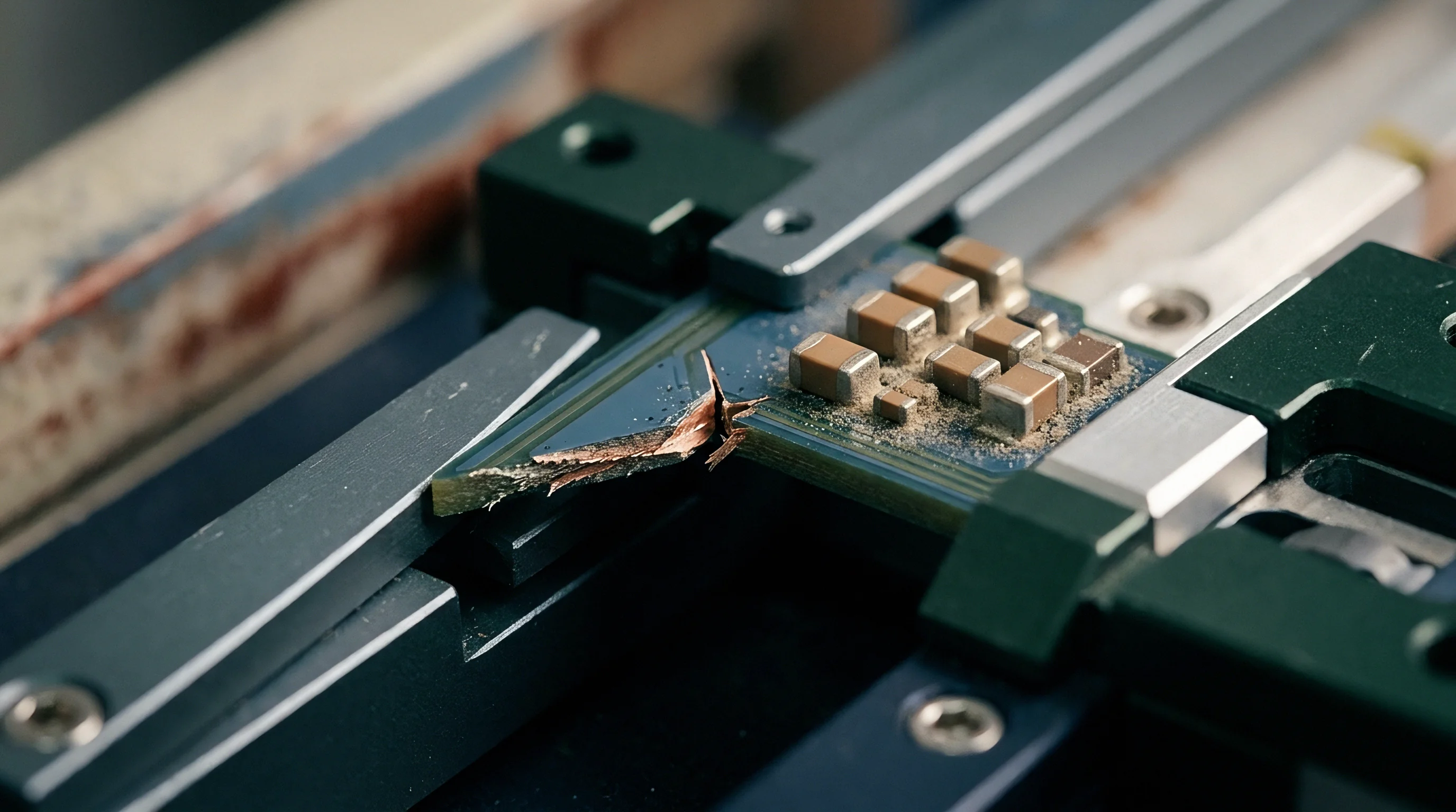
CAF pathways form micro-conductive threads along glass weave bundles beneath RF microstrip traces. As filaments approach signal traces, local electric field density increases exponentially. Localized dielectric breakdown occurs before complete metallic shorting, causing intermittent phase noise, elevated signal attenuation, and localized dielectric heating.
High bias voltages on power amplifier supply lines adjacent to sensitive RF interconnects accelerate filament growth velocity.

Polymeric Chain Scission and Glass-Weave Micro-Cracking
Repeated thermal expansion mismatch between woven fiberglass bundles and surrounding resin fractures chemical bonds at the interface. Polymer chains scission under heat. Fiberglass exhibits a coefficient of thermal expansion around five parts per million per degree Celsius, whereas epoxy resin expands at sixty parts per million per degree Celsius below glass transition temperature.
Operating temperature swings generate mechanical shear stress along interface boundaries.
Micro-cracking along glass weave bundles introduces air gaps with a dielectric constant of one point zero. The localized reduction in permittivity shifts line impedance upward, creating periodic impedance discontinuities along long interconnect traces. Periodic micro-cracks behave like Bragg reflectors at millimeter-wave frequencies, creating narrow stopbands that abruptly block signal transmission at specific frequencies.
Consider a 10 cm microstrip transmission line operating inside an unsealed industrial gateway. Initial board parameters at 20 degrees Celsius and 30 percent relative humidity yield a dielectric constant of 4.20 and a loss tangent of 0.012 on high-Tg FR-4. At 2.4 GHz, conductor loss measures 0.12 dB/cm and dielectric loss measures 0.08 dB/cm, yielding a baseline total insertion loss of 2.0 dB across the 10 cm interconnect.
After three years of continuous operational exposure to 60 degrees Celsius and 85 percent relative humidity under DC bias, substrate degradation shifts parameters. Moisture absorption elevates the effective dielectric constant to 4.55 and increases loss tangent to 0.028 through polymer hydrolysis and dipole relaxation. Hydrolysis and micro-cracking add 0.04 dB/cm to conductor loss from surface oxide growth, while dielectric loss increases from 0.08 dB/cm to 0.21 dB/cm.
αdielectric, aged = fracπ · (2.4 × 10⁹) · sqrt4.553 × 108 · 0.028 = 4.86 Np/m = 0.21 dB/cm
Total interconnect insertion loss rises from 2.0 dB to 3.7 dB. A 1.7 dB loss increase directly consumes transmitter output power. In a BLE link with 0 dBm transmit power and -93 dBm receiver sensitivity, a 1.7 dB line loss increase reduces operating range by approximately nineteen percent in an open line-of-sight environment, assuming a path loss exponent of 2.1.
| Frequency Band | Initial Loss (dB/cm) | Aged Loss (dB/cm) | Dielectric Shift (Δ varεr) | Loss Tangent Shift (Δ tanδ) | Link Margin Impact |
|---|---|---|---|---|---|
| 868 / 915 MHz | 0.04 | 0.06 | +0.25 | +0.0050 | -0.2 dB over 10 cm |
| 2.4 GHz ISM | 0.20 | 0.37 | +0.35 | +0.0160 | -1.7 dB over 10 cm |
| 5.8 GHz ISM | 0.55 | 1.15 | +0.40 | +0.0220 | -6.0 dB over 10 cm |
| 24 GHz ISM | 1.80 | 4.20 | +0.45 | +0.0280 | -24.0 dB over 10 cm |
RF insertion loss doubles whenever ambient humidity hydrolyzes the epoxy resin boundary along a microstrip conductor.
Verifying substrate longevity requires subjecting test coupons to standardized accelerated environmental stress procedures before releasing production layout designs.
- Precondition unpopulated circuit test coupons at 105 degrees Celsius for 24 hours to drive out residual manufacturing moisture and establish absolute dry baseline weights.
- Measure baseline S21 insertion loss and phase delay across target operating frequencies using a calibrated vector network analyzer and microstrip test fixtures.
- Transfer coupons into an environmental chamber set to 85 degrees Celsius and 85 percent relative humidity with a continuous 50-volt DC bias applied across trace-to-ground gaps.
- Extract test coupons at 250, 500, and 1000-hour intervals, performing immediate vector network analyzer measurements within fifteen minutes of chamber removal.
- Bake coupons at 105 degrees Celsius for 24 hours post-test to isolate permanent chemical resin degradation from reversible absorbed moisture effects.
Failing to account for substrate dielectric decay results in continuous field return rate growth as deployed radios slowly drop off wireless networks due to accumulating interconnect loss.

Bench
Quantifying high-frequency attenuation shifts requires precise vector measurement setups isolated from thermal fluctuations. High-frequency vector network analyzers evaluate transmission line performance by measuring four-port scattering parameters. Refinement requires clean calibration.
Direct measurement of microstrip structures includes loss contributions from coaxial connectors, launch transitions, and cable assemblies that mask underlying substrate absorption changes.
Accurate parameter extraction relies on de-embedding techniques that mathematically subtract test fixture artifacts from raw measured data. Thru-Reflect-Line (TRL) calibration places reference planes directly on the printed circuit board substrate, eliminating SMA launch loss and phase shifts. Attenuators stabilize port reflections.
Isolated substrate measurements distinguish conductor copper loss from dielectric dissipation factor changes across temperature and humidity cycles.
Vector Network Analyzer De-Embedding Techniques
Accurate extraction of dielectric loss tangent requires removing fixture transition artifacts from raw scattering parameters. Standard Short-Open-Load-Through (SOLT) calibration moves reference planes to coaxial cable ends, leaving printed circuit board edge-launch connectors inside the measurement loop. Edge-launch transitions introduce capacitive discontinuities that distort high-frequency S11 return loss curves.
TRL calibration utilizes printed microstrip standards manufactured on the exact substrate material under test. The Thru standard sets zero reference length, the Reflect standard provides high reflection coefficient, and the Line standard establishes ninety-degree phase delay at center frequency. Implementing TRL calibration shifts reference planes directly onto the microstrip trace, isolating dielectric loss tangent extraction from connector contact resistance and PCB launch step discontinuities.

Does Humidity Shift Microstrip Insertion Loss?
Environmental test chambers pair vector instruments with controlled ambient conditioning to isolate material attenuation drift. Test coupons featuring long meandered microstrip lines, differential pairs, and resonant ring structures reside inside the chamber while RF low-loss phase-stable cables pass through bulkhead ports to external measurement instruments. Real-time vector monitoring tracks insertion loss escalation as humidity levels transition from ten percent to ninety percent relative humidity.
Resonant ring structures offer accurate dielectric loss tangent measurement without requiring precise physical line length knowledge. The quality factor of the ring resonator depends on total circuit losses. As substrate dissipation factor elevates under moisture absorption, ring resonance curves broaden and peak amplitude drops.
Calculating the loaded quality factor at resonant peak frequencies reveals exact relative permittivity and loss tangent shifts without de-embedding coaxial launch transitions.
Microstrip resonant ring circuits isolate dielectric relaxation shifts without conductor surface roughness masking the absorption loss.
Rigorous substrate selection requires evaluating key material characteristics through bench test verification protocol checklists:
- Permittivity Tolerance Verification confirms lot-to-lot dielectric constant variation stays within engineered matching limits across full production volumes.
- Moisture Absorption Rate Testing measures percentage weight gain and corresponding S21 attenuation increase after 500 hours of saturated steam exposure.
- Thermal Dissipation Factor Drift plots loss tangent changes from minus 40 degrees to plus 125 degrees Celsius to establish thermal operating margins.
- Copper Adhesion Peel Strength verifies mechanical foil bond integrity after 1000 hours of high-humidity thermal aging to prevent trace lifting.
- CAF Resistance Qualification monitors leakage current across 100-micron trace spacing under 100-volt continuous bias for 1000 hours.
Can advanced surface hydrophobic coatings fully seal porous substrate edges against ambient moisture ingress without introducing high-frequency dielectric loading losses of their own?


Provision
Long-term RF link integrity requires explicitly accounting for material degradation during the initial component selection phase. Module designers who rely solely on room-temperature dry-substrate datasheets risk under-specifying link margins. Laminate selection dictates link life.
Integrating a two-decibel aging margin into system-level link budget calculations protects communication range across five-to-ten-year product operational lifespans in unconditioned outdoor enclosures.
Strategic bill of materials engineering balances raw substrate cost against long-term maintenance liabilities. High-frequency RF sections can be isolated onto dedicated low-loss sub-module daughtercards using hydrocarbon or LCP materials, while baseband digital processing remains on standard low-cost FR-4 mainboards. Hybrid multilayer PCB stackups combine thin low-loss outer RF dielectrics with thick conventional FR-4 inner cores, optimizing high-frequency transmission performance while maintaining structural rigidity and mechanical economy.
Link Budget Degradation Allocations in RF Procurement
Transmitter output power and receiver sensitivity establish the initial operational boundaries of any wireless link. Sourcing teams specify acceptable interconnect loss limits within module procurement contracts to prevent field failures caused by substrate aging. The link budget allocation assigns specific decibel losses to trace attenuation, connector interfaces, filter insertion loss, and environmental fade margin.
PRX = PTX + GTX + GRX – Lpath – Linterconnect – Laging
Where Laging accounts for substrate dielectric dissipation degradation over expected operating life. Allocating 1.5 dB to 3.0 dB for substrate degradation ensures receiver sensitivity thresholds remain unviolated when humidity and thermal stress elevate dielectric loss tangent in mature field deployments.

Laminate Qualification Metrics in Commercial RFQs
Purchasing agreements for high-frequency circuit materials specify strict initial dielectric constant tolerances. Request for Quote (RFQ) documentation must require suppliers to submit IPC-4101 test reports covering moisture absorption, thermal expansion coefficients, and dissipation factor stability over temperature. Sourcing engineers enforce incoming lot inspection testing using microstrip resonant coupons to verify material compliance before board fabrication.
| Substrate Class | Optimal RF Band | 10-Year Loss Drift (dB/m @ 2.4 GHz) | Relative Laminate Cost | Target Application |
|---|---|---|---|---|
| Standard FR-4 | Sub-1 GHz | +15.0 | 1.0x | Cost-sensitive Smart Metering |
| High-Tg FR-4 | 2.4 GHz ISM | +8.5 | 1.3x | Indoor Industrial IoT Gateways |
| Enhanced Hydrocarbon | 5.8 GHz / Wi-Fi 6 | +1.2 | 2.8x | Outdoor Wi-Fi / Cellular Small Cells |
| PTFE / Microfiber | 24 GHz / 60 GHz Radar | +0.4 | 5.5x | Automotive Radar / MmWave Backhaul |
| LCP Thin Film | Flexible RF Arrays | +0.3 | 7.0x | High-Density Wearable / Medical Radios |
RF interconnect loss scales inversely with material investment, where paying a three-fold laminate price premium eliminates ninety percent of long-term environmental link margin degradation.