Meaning
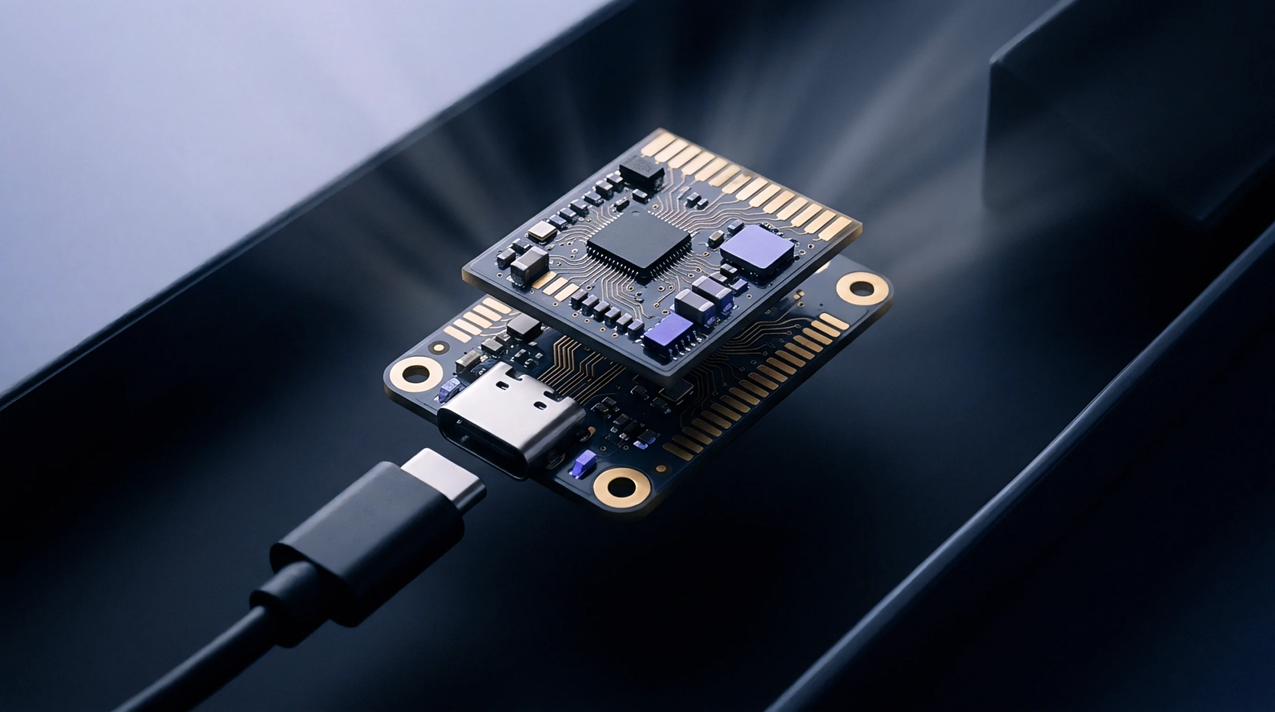
Lithographic reduction is the reduction of printed gate lengths and metal pitches inside a semiconductor manufacturing line to increase transistor density per square millimeter of silicon. When fabrication plants implement a die shrink, the physical dimensions of every circuit element scale downward by a constant factor. This geometrical compression alters the resistance and capacitance profile of local interconnects, which changes signal propagation delays across the substrate.
Component engineers measure the success of this scaling by counting functioning transistors within a fixed reticle field. The boundary of this definition sits at the mask level, so architectural reorganizations that move blocks around without shrinking transistors fall outside the category.
Lithographic Scaling
Photomasks project shorter wavelengths of ultraviolet light through complex optical correction systems to pattern features that are smaller than the light wavelength itself. Immersion lithography introduces purified water between the final lens element and the photoresist to increase the numerical aperture of the exposure tool. Extreme ultraviolet scanners replace refractive lenses with multilayer mirrors to handle the absorption losses inherent in very short photon streams.
Etching chambers then remove unprotected silicon dioxide layers using reactive plasmas tailored to anisotropic profiles. Each mask layer must maintain strict overlay tolerances to prevent electrical shorts between adjacent metal contacts on the board.
Thermal Budget
Smaller transistor geometries pack higher power dissipation into localized hot spots because current density rises faster than surface area decreases. Foundry packaging teams apply finite element analysis to model heat transfer through copper pillars and thermal interface materials. Thinner silicon dies crack easily during wire bonding operations if thermal expansion coefficients mismatch between the chip carrier and the printed circuit board.
Higher operating temperatures accelerate electro-migration inside narrow copper interconnects, shortening the operational lifespan of the final connectivity module. System integrators manage this reality by throttling clock speeds when thermal sensors report junction temperatures exceeding safe thresholds.
Electrical Qualification
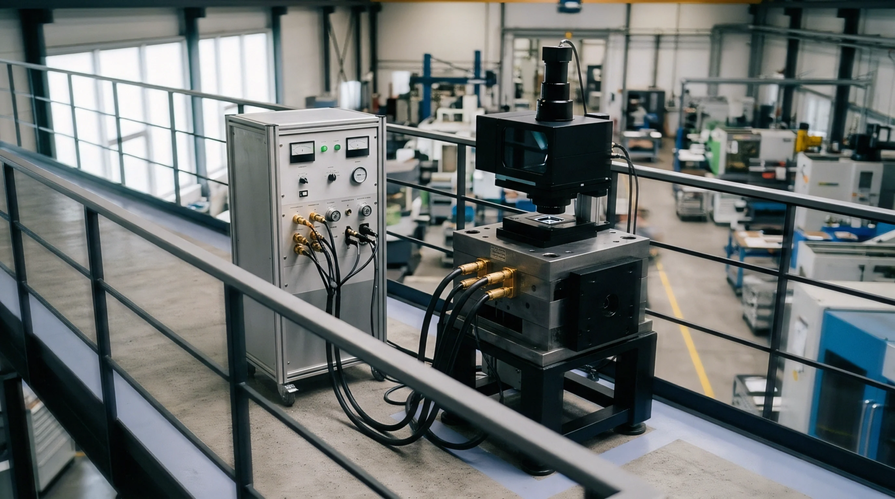
Qualification tests subject the scaled semiconductor to accelerated aging at elevated voltages to screen for gate oxide breakdown and hot carrier injection. Buyers run these samples through rigorous radio frequency compliance checks to verify that parasitic capacitances do not degrade receiver sensitivity in mobile handsets. Test sockets on the automated production line must accommodate smaller pin pitches without introducing contact resistance variations that skew analog measurements.
Production yields stabilize only after engineers adjust the burn-in voltage profiles to match the electrical characteristics of the smaller fabrication node. Long term reliability depends on maintaining consistent packaging stress limits throughout the assembly lifecycle.