Electromagnetic Absorption Characteristics of Conductive Polymer Composites
Conductive polymer composite absorption depends on balancing complex permittivity and skin depth to eliminate surface reflection and satisfy radiated emission limits.


Percolation
When high-frequency energy strikes a synthetic matrix, attenuation comes down to complex permittivity, intrinsic electrical conductivity, and internal wave reflections. In conductive polymer composites, dissipation works through two distinct channels: real permittivity, which governs charge storage capacity, and imaginary permittivity, which handles dielectric loss. Base polymers such as polypropylene, polyamide, and polycarbonate carry virtually no inherent conductivity, leaving them transparent to radio signals.
Dispersing conductive nanofillers into these insulating matrices alters their high-frequency response once the volume fraction crosses a critical threshold.
At low filler loadings, isolated conductive particles remain separated by wide gaps of polymer. Electromagnetic waves pass through with negligible ohmic loss, relying only on weak dipoles along the polymer backbone to dissipate energy. As filler concentration rises, the average distance between particles shrinks until electron hopping and tunneling create localized current paths.
The point where continuous paths form through the three-dimensional volume marks the transition from insulating behavior to conductive dissipation. Beyond this threshold, real permittivity jumps and imaginary permittivity climbs by orders of magnitude, turning the composite into an effective electromagnetic absorber.
The dielectric loss tangent of a multi-walled carbon nanotube composite loaded at two weight percent reaches zero point four five at eight gigahertz under room temperature testing.
Shielding performance in conductive polymers depends on balancing internal attenuation against surface reflection. High surface conductivity reflects incoming waves back toward the source, much like a conventional metallic enclosure. While pure reflection keeps interference away from internal electronics, it bounces stray radiation into surrounding equipment.
Controlled absorption, by contrast, dissipates energy inside the bulk material, converting high-frequency waves into heat through electron scattering and dipole relaxation. Making absorption dominant requires matching wave impedance at the interface so incoming waves enter the material rather than bouncing off the surface.
Impedance matching requires the absorber’s characteristic impedance to match that of free space, which sits at roughly three hundred seventy-seven ohms. When a wave hits a material where complex dielectric permittivity far outweighs complex magnetic permeability, surface impedance drops well below free space and causes heavy front-face reflection. Adding magnetic nanoparticles like nickel-zinc ferrites or carbonyl iron to the matrix pulls complex permeability upward.
Raising both the real and imaginary components of magnetic permeability balances the refractive index, allowing high-frequency waves to pass deep into the lossy composite where conductive networks absorb them.
A composite’s skin depth determines how thick it must be to hit target attenuation levels. Calculated as the inverse square root of the product of pi, operating frequency, magnetic permeability, and bulk conductivity, skin depth drops rapidly as frequencies reach the gigahertz range. At lower ISM frequencies like thirteen point five six megahertz or nine hundred megahertz, skin depth in moderately conductive polymers spans several millimeters, so absorbing radiation takes thick walls.
At millimeter-wave bands like twenty-four or sixty gigahertz, skin depth drops below one hundred micrometers, meaning thin films and surface coatings can deliver significant attenuation.
A 14 dB divergence in shielding effectiveness occurred across a single injection-molded batch when filler dispersion varied by three percent.

Dielectric Dissipation Pathways and Complex Permittivity Dynamics
Energy transfer from an electromagnetic wave into a conductive matrix relies on microscopic polarization. Electronic polarization happens quickly as electron clouds shift against atomic nuclei in alternating electric fields. Atomic polarization involves the displacement of atoms within chemical bonds and remains effective into the infrared spectrum.
Interfacial polarization ~ often called Maxwell-Wagner-Sillars relaxation ~ takes place at structural boundaries inside heterogeneous composites. As charge carriers move with the high-frequency field, they gather at boundaries between conductive fillers and insulating polymer chains, forming macro-dipoles that absorb radiation through relaxation losses.
The relaxation time of interfacial polarization determines the frequency band where dielectric loss peaks. If field frequency exceeds the inverse of this relaxation time, accumulated charges can no longer keep up with the field reversals, driving up imaginary permittivity. Combining high-aspect-ratio carbon nanotubes with planar graphene flakes creates hybrid filler networks with multiple relaxation frequencies across broad radio bands.
This multi-tiered structure widens the absorption band so narrow operational drops don’t compromise shielding integrity.
| Filler Material | Aspect Ratio (L/D) | Percolation Weight % | Real Permittivity (ε’) | Imaginary Permittivity (ε”) | Skin Depth at 10 GHz (mm) |
|---|---|---|---|---|---|
| Multi-Walled Carbon Nanotubes | 1000 to 1500 | 0.5 to 1.5 | 14.2 | 5.8 | 0.85 |
| Graphene Nanoplatelets | 200 to 500 | 1.0 to 2.5 | 11.6 | 3.4 | 1.12 |
| Polyaniline Nanofibers | 20 to 50 | 3.0 to 8.0 | 6.5 | 1.9 | 2.40 |
| MXene Titanium Carbide Sheets | 500 to 800 | 0.8 to 2.0 | 18.4 | 8.1 | 0.42 |
| Carbonyl Iron Powder | 1 to 5 | 15.0 to 40.0 | 8.1 | 0.6 | 1.85 |
Polyaniline, polypyrrole, and poly(3,4-ethylenedioxythiophene) doped with polystyrene sulfonate are intrinsically conductive polymers whose charge carriers consist of polarons and bipolarons. Unlike passive carbon fillers, these conjugated polymer chains conduct electricity along their backbones through delocalized pi-electron systems. Counter-ion doping controls carrier density, allowing precise tuning of imaginary permittivity without altering structural viscosity.
Blending these conductive polymers into structural resins like ABS or nylon yields homogeneous absorbing materials that avoid the agglomeration problems typical of carbon black.
How conductive fillers align during processing heavily influences anisotropic absorption. Extrusion and injection molding expose molten polymer blends to high shear forces near tool surfaces, lining up high-aspect-ratio fibers parallel to mold walls. Fields polarized parallel to this orientation hit low-resistance paths and reflect heavily off the surface.
Fields polarized perpendicular to the fiber alignment penetrate deeper into the substrate before being absorbed. Tool designers have to adjust gate locations and injection speeds to control flow fronts, avoiding directional shielding weaknesses in finished enclosures.

Magnetic Coupling Mechanics and Impedance Matching Optimizations
Permeability matching is the primary way to reduce front-surface reflection in microwave absorbers. Pure dielectric composites have high complex permittivity but near-unity complex permeability, giving them an intrinsic impedance well below free space. When an incoming wave hits this impedance step, reflection rises according to boundary field continuity equations.
Adding ferromagnetic nanofillers introduces complex permeability to the composite tensor, narrowing the gap between dielectric and magnetic responses.
Magnetic losses come from domain wall resonance, natural ferromagnetic resonance, and eddy current dissipation. Below two gigahertz, domain wall movement accounts for most magnetic energy loss. Above two gigahertz, natural ferromagnetic resonance dominates, driven by the magnetocrystalline anisotropy field of the magnetic phase.
Hexagonal ferrites and iron-alloy nanoparticles have high anisotropy fields that push natural resonance up into X-band and Ku-band frequencies. By tuning the ratio between carbon dielectric fillers and ferrite magnetic fillers, engineers can design absorption layers with minimal reflection at specific radar and cellular bands.
Eddy currents inside conductive magnetic inclusions create another dissipation channel. Alternating magnetic fields induce local circular currents within individual metal particles. If particle diameters exceed the magnetic skin depth, internal eddy currents generate opposing fields that shield the particle interior, dropping effective permeability.
Keeping ferromagnetic particle sizes below fifty nanometers suppresses this bulk shielding while maximizing surface spin-relaxation loss, maintaining high imaginary permeability across wide gigahertz bands.
How does filler geometry alter the balance between surface reflection and volumetric absorption in ultra-thin composite housings?
Foil
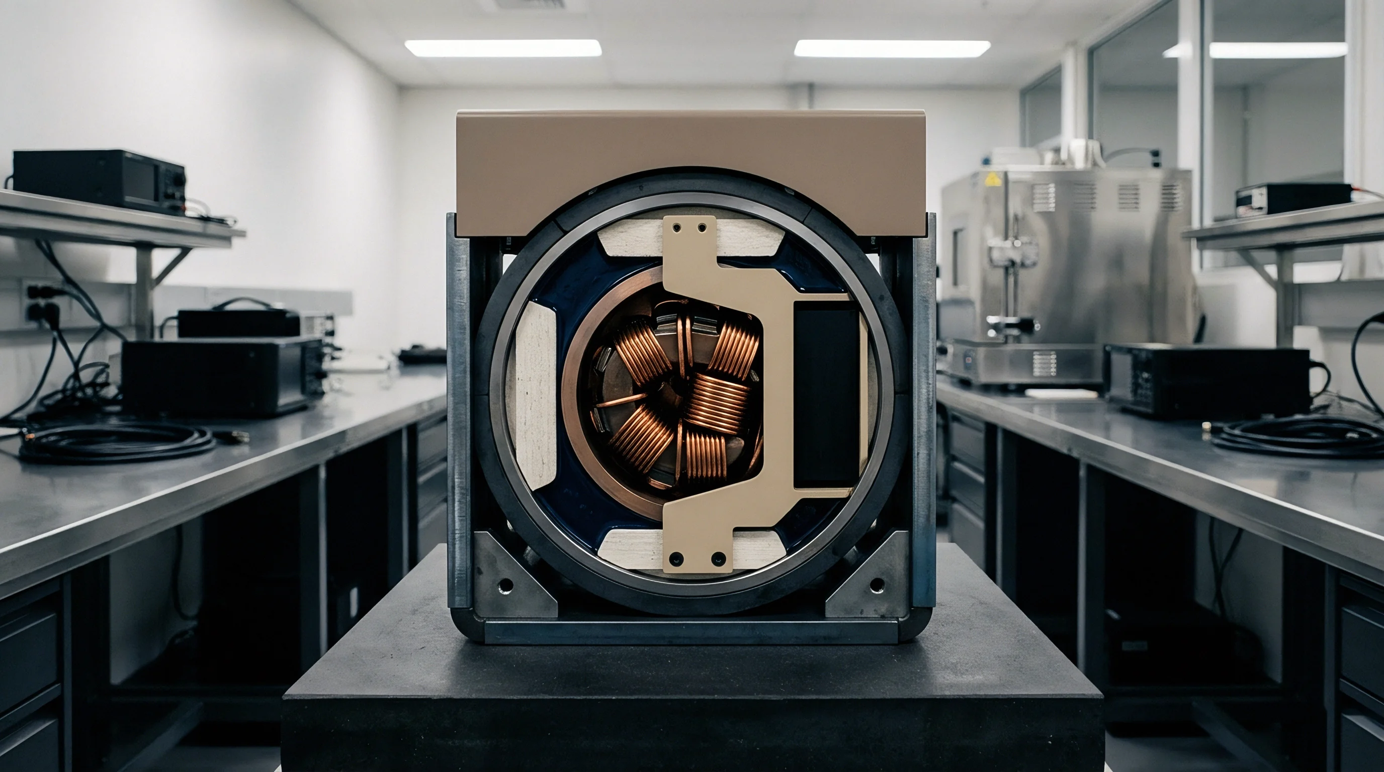
Testing attenuation in planar conductive polymer composites requires standardized coaxial fixtures. ASTM D4935 defines the benchmark method for measuring shielding effectiveness in planar materials using a displaced inner conductor holder. Test specimens consist of a reference ring and a solid disc cut from the same sheet stock.
The fixture creates a transverse electromagnetic wave environment up to one point five gigahertz, separating intrinsic material losses from edge diffraction and aperture leakage typical of cabinet-level testing.
Measuring performance across higher microwave bands ~ between eight gigahertz and forty gigahertz ~ requires rectangular waveguides or free-space quasi-optical setups. Waveguide testing uses precisely machined composite plugs fitted inside metallic waveguide sections, with vector network analyzers gathering two-port scattering parameters. S11 represents the input reflection coefficient, and S21 measures forward transmission.
Mathematical inversion then extracts intrinsic complex permittivity and permeability from these S-parameters, yielding material properties independent of sample geometry.
Dual-port vector network analyzer scans verified the complex permittivity tensor components.
Extracting dielectric properties from measured S-parameters typically relies on the Nicolson-Ross-Weir algorithm, which converts phase and magnitude data into real and imaginary material constants. When sample thickness matches integer multiples of half the wavelength inside the material, S11 drops toward zero, causing phase singularities in the extraction math. Test engineers avoid this half-wavelength divergence by running samples of different thicknesses or using non-iterative approaches like the NIST precision polynomial model.
Measurement errors in coaxial and waveguide setups usually come from sample defects or air gaps along fixture walls. A gap of just fifty micrometers between the sample edge and the metal waveguide wall creates a capacitive leakage path with lower impedance. Radiation bypasses the material entirely through this edge gap, artificially dropping measured absorption loss by up to twenty decibels.
Cutting test plugs with lasers or cryogenic milling keeps tolerances within five micrometers, ensuring tight contact against cell walls.
Standard ASTM D4935 testing requires a reference and load specimen pair machined from the same production lot within a thickness variation limit of ten micrometers.
Free-space methods avoid wall-contact issues altogether by focusing microwave energy onto composite panels with lens-fitted horn antennas. A quasi-optical free-space setup places a flat panel between transmitting and receiving antennas inside an anechoic chamber. Time-domain gating on the vector network analyzer isolates main reflections at the sample interface from room reflections and edge diffraction.
This approach also allows temperature-dependent testing, evaluating panels under realistic thermal profiles from minus forty degrees Celsius up to eighty-five degrees Celsius.
Receiving inspection rejected two carrier shipments of high-density polyethylene loaded with multi-walled carbon nanotubes after bench verification revealed non-uniform resistivity.

Nicolson-Ross-Weir Extraction Protocols and Waveguide Boundary Control
Repeatable material characterization depends on precise calibration of the vector network analyzer. Short-Open-Load-Thru calibration sets reference planes at coaxial connector tips, while Thru-Reflect-Line calibration places reference planes inside waveguide holders. Phase shifts caused by cable flex or temperature shifts introduce serious error into imaginary permittivity calculations.
Labs should verify calibration stability with a certified Teflon slab before running formal compliance scans on polymer batches.
Surface roughness alters front-face reflection during high-frequency waveguide testing. When surface irregularities approach the size of the internal wavelength, specular reflection shifts to diffuse scattering. Scattered waves bounce off waveguide walls at oblique angles, exciting higher-order non-TEM modes.
These modes decay rapidly and register at the receiving port as artificial material absorption. To protect measurement integrity, molds used for test slabs need an optical mirror finish with average roughness below zero point two micrometers.
- Specimen Dimensioning requires cutting flat test slabs to match exact waveguide internal cross-sections, holding tolerances within plus or minus five micrometers using CNC cryogenic milling.
- Fixture Cleaning involves wiping silver-plated internal waveguide walls with electronic-grade isopropyl alcohol to remove skin oils, oxidation, and residue before inserting samples.
- Sample Alignment positions the face of the polymer composite specimen perpendicular to the waveguide’s longitudinal axis to prevent phase front distortion during S-parameter measurements.
- VNA Calibration runs a full two-port Thru-Reflect-Line calibration across the target frequency band, setting reference planes directly at the sample faces.
- S-Parameter Acquisition records magnitude and phase data for S11, S21, S12, and S22 across one thousand six hundred one discrete frequency points under stable laboratory conditions.
- Property Inversion processes raw scattering matrices with non-iterative numerical algorithms to calculate complex permittivity, complex permeability, and total shielding effectiveness.
Sample thickness directly affects the accuracy of calculated loss tangents. Very thin specimens under one hundred micrometers show minimal phase shift, leaving phase noise to dominate extraction algorithms. Overly thick specimens drop S21 signals into the analyzer’s noise floor, losing the dynamic range needed to resolve imaginary permittivity.
Ideal sample thickness keeps total forward transmission loss between ten and forty decibels across the measured band, balancing phase resolution against signal-to-noise limits.

Free-Space Quasi-Optical Setup and Anisotropy Detection
Evaluating non-homogeneous composite panels with woven conductive fibers requires polarized free-space benches. These setups mount horn antennas on rotation stages, stepping linear polarization from zero to three hundred sixty degrees relative to the material axis. Rotating the polarization vector maps anisotropic absorption tensors, uncovering directional shielding weak spots tied to fiber alignment.
Automated motion controllers turn the sample holders while keeping focal distances precise, preserving phase plane consistency across rotational scans.
| Measurement Method | Frequency Range | Sample Geometry | Primary Advantage | Primary Limitation |
|---|---|---|---|---|
| ASTM D4935 Coaxial Cell | 30 MHz – 1.5 GHz | Displaced ring and disc planar specimen | Standardized baseline for TEM absorption | Upper frequency limited by higher-order modes |
| Rectangular Waveguide | 1.7 GHz – 110 GHz | Precision machined rectangular plug | High dynamic range for S-parameter extraction | Extreme sensitivity to wall air gaps |
| Resonant Cavity Perturbation | 1 GHz – 20 GHz | Small rod or thin strip specimen | Exceptional sensitivity for low-loss materials | Single-frequency discrete measurements only |
| Quasi-Optical Free-Space | 8.2 GHz – 320 GHz | Large flat panel (150mm x 150mm minimum) | Non-destructive, temperature-controlled testing | Requires complex time-domain gating and calibration |
Temperature-dependent measurements require placing environmental chambers with RF-transparent windows into the quasi-optical beam path. Polymer matrices alter their conductivity as temperature moves from sub-zero conditions up to high operating levels. Thermal expansion increases the space between carbon fillers, weakening conductive tunneling paths and reducing imaginary permittivity.
Tracking temperature-driven shielding decay helps prevent field failures in automotive radar housings and aerospace enclosures subject to severe thermal cycling.
A calibration error on the laboratory vector network analyzer delayed sample verification by two weeks and destroyed three batch development schedules.


Attenuation
Using conductive polymer composites in commercial enclosures replaces traditional stamped metal shields, saving weight and simplifying high-volume assembly. Housings modified with conductive fillers still have to meet global radiation limits set by regional regulators. In the US, FCC Part 15 Subpart B sets field strength limits for unintentional radiators.
In Europe, the Radio Equipment Directive requires testing against harmonized standards like ETSI EN 301 489-1 for general EMC and ETSI EN 300 328 for wideband data equipment operating in the two point four gigahertz band.
Conductive polymer enclosures have to suppress both near-field reactive coupling from circuit board traces and far-field emissions from high-speed internal buses. Plain plastic lets RF noise radiate unchecked, missing Class B commercial emission limits by a wide margin. Switching to a composite housing loaded with three weight percent graphene nanoplatelets reduces internal emissions by thirty-five decibels across the X-band.
That level of absorption keeps unwanted harmonics below regulatory ceilings without needing extra metal ground planes or sprayed conductive coatings.
Unshielded plastic housing retrofits caused secondary harmonic scan failures during laboratory testing of commercial RF filings.
Submitting an electronic product for radio approval means documenting housing compliance in the technical construction file. Certification bodies look for proof that housing changes don’t compromise spectrum integrity or thermal safety. Standard IEC 62368-1 covers audio, video, and IT equipment, setting strict mechanical and flammability rules for plastic enclosures.
Adding carbon black or metallic nanofillers alters UL 94 flammability ratings, often dropping a base resin from V-0 self-extinguishing status down to V-2. Engineers have to check that filler additives don’t void safety certificates while chasing EMC approval.
Modular radio approvals bring specific integration constraints when used with absorbing housings. A pre-certified radio module holds a grant based on testing inside an open-air reference host. Put that module inside a high-absorption composite shell, and you alter the antenna’s radiation pattern, gain, and total radiated power.
Excessive housing absorption drops output power and hurts link budget. If the housing detunes the antenna, impedance mismatch reflects power back into the amplifier, generating spurious emissions that violate FCC Part 15.247 band-edge rules.
The European Telecommunications Standards Institute standard EN 301 489-1 limits radiated spurious emissions from electronic enclosures to forty dBuV/m measured at a three-meter distance across the one to six gigahertz band.
Dynamic Frequency Selection rules under FCC Part 15 Subpart E and ETSI EN 301 893 add challenges for absorbing housings on five gigahertz Wi-Fi devices. Products operating in radar-sharing bands have to detect incoming radar signals down to minus sixty-two dBm. If an absorbing enclosure attenuates those radar pulses before they reach the antenna chip, receiver sensitivity drops.
The device then fails compliance by continuing to transmit on channels used by weather radar, blocking market access until the housing’s absorption profile is adjusted around the antenna.
Antenna detuning is a main failure point when integrating absorbing polymer covers into hosts. Placing a lossy conductive composite in the reactive near-field of an inverted-F or patch antenna pulls the resonant frequency down and expands real input impedance. Near-field absorption turns radiated power straight into heat, dropping radiation efficiency below forty percent.
Manufacturers have to keep clear exclusion zones around integral antennas, using unfilled polymer windows over radiator apertures and limiting absorbing composites to noise-heavy processing areas.

Harmonic Suppression and Spurious Emission Mitigation
Modern system-on-chip processors run data buses at high harmonics that radiate narrow spikes across wide bands. Metal shields reflect these spikes around cabinet cavities, building up energy until it leaks through seams or cable entry points. Conductive polymer absorbers act as local high-frequency dampers, absorbing cavity resonance without causing standing wave reflections.
Placing molded baffles over high-speed memory buses lowers cavity Q-factors, cutting radiated emissions at seam apertures by twelve to eighteen decibels.
Compliance chambers measure radiated emissions on motorized turntables at three- or ten-meter distances. As the product turns three hundred sixty degrees, receiving antennas move between one and four meters to search for emission peaks. Conductive polymer enclosures with isotropic absorption produce flat radiation profiles during rotation, avoiding the sharp directional lobes common with seam-leaking metal covers.
This uniform attenuation speeds up scan times, cutting expensive lab hours during certification campaigns.
- 1. Baseline Pre-Scan Execution maps the unshielded circuit board’s radiated spectrum inside a semi-anechoic chamber from thirty megahertz to forty gigahertz using a spectrum analyzer with peak hold.
- 2. Hotspot Identification locates high-frequency leakage zones on the host assembly using near-field magnetic probes connected to a high-bandwidth oscilloscope.
- 3. Composite Shield Selection matches candidate polymer loss tangent peaks to the noise frequencies identified during near-field probing.
- 4. Housing Aperture Sealing uses conductive elastomeric gaskets along tongue-and-groove joints to stop slot-line radiation from bypassing absorbing composite walls.
- 5. Radiated Spurious Measurement runs compliance sweeps under ANSI C63.4 procedures, confirming peak and average field strengths stay six decibels below regulatory limits.
- 6. Antenna Pattern Verification captures 3D spherical gain maps inside a fully anechoic OTA chamber to verify spatial radiation efficiency stays within approved limits.
Permissive change rules dictate whether changing enclosure materials requires full re-certification. Under FCC regulations, a Class I Permissive Change covers minor modifications that don’t degrade radiated emissions. Replacing a metal shield with a conductive polymer alters radiated field dynamics, forcing engineers to file a Class II Permissive Change.
That filing requires submitting chamber test data, updated photos, and a revised operational description to a Telecommunications Certification Body before units can ship.

Antenna Near-Field Interference and Specific Absorption Rate Compliance
Placing conductive absorbing composites near body-exposure zones alters Specific Absorption Rate (SAR) performance in portable products. FCC Part 2.1093 and IEC/IEEE 62209-1528 govern RF exposure from devices operating within twenty centimeters of a user’s head or body. When a portable transmitter runs next to the body, backward radiation from internal antennas deposits energy directly into biological tissue.
Adding a thin conductive polymer absorbing layer behind the antenna array redirects radiation away from the user, lowering localized 1g or 10g peak SAR values to meet exposure limits.
At high operating frequencies, skin depth drops dramatically.
Designing absorption layers for SAR reduction requires careful dielectric constant matching. If the composite layer’s dielectric constant is too high, near-field reactive coupling increases, drawing power out of the antenna into heat inside the housing. An effective SAR absorption layer uses a graded-index architecture: a low-permittivity dielectric buffer sits next to the antenna, backed by a high-loss carbon nanotube composite layer facing the outer case.
This arrangement matches near-field impedance while absorbing the backward radiation lobe before it reaches human tissue.
Modifying enclosure housing materials under European Telecommunications Standards Institute rules requires updating the formal Declaration of Conformity under RED Article 3.1b and Article 3.2.
Landed
Moving conductive polymer formulations from lab synthesis to high-volume injection molding introduces major cost and supply chain challenges. Base structural resins like ABS or polybutylene terephthalate cost two to four US dollars per kilogram. Loading them with multi-walled carbon nanotubes, graphene nanoplatelets, or MXenes drives compound prices up to fifty to two hundred fifty US dollars per kilogram.
High raw material costs make wall-thickness optimization critical during design to reduce shot weight while meeting attenuation requirements.
Tool wear is an easily overlooked operating expense when molding abrasive conductive fillers. Carbon fibers, metallic flakes, and ceramic ferrite particles wear down hardened steel molds, eroding gates and runners. Standard molds rated for one million cycles in unfilled polypropylene can show gate erosion after fifty thousand cycles when running thirty percent nickel-coated carbon fiber.
Tool wear increases part wall dimensions, changing cavity volumes and shifting shear alignment, which causes batch-to-batch drift in shielding effectiveness.
Compliance testing inside anechoic chambers consumes substantial billable hours.
Procuring pre-compounded conductive resin pellets requires strict receiving inspections. Supplier certificates of analysis usually report bulk DC volume resistivity measured under ASTM D257, but DC resistivity correlates poorly with gigahertz absorption loss. A batch with low DC resistance can easily fail high-frequency attenuation targets if filler agglomeration disrupts interfacial polarization.
Incoming quality teams should run RF batch checks using coaxial fixture tests on molded sample disks before releasing resin to production.
| Regulatory Jurisdiction | Mandatory Standard | Required Test Samples | Typical Filing Lead Time | Retest Exposure Risk | In-Country Agent Mandate |
|---|---|---|---|---|---|
| United States (FCC) | FCC Part 15 Subpart B / C | 2 complete final hosts | 3 to 5 weeks | Medium (Spurious band-edge failures) | Required (US Agent for Service) |
| European Union (CE) | EN 301 489 / EN 300 328 | 3 complete final hosts | 4 to 6 weeks | High (Immunity & harmonic limits) | Required (EU Authorised Rep) |
| Japan (MIC / Giteki) | Radio Law Article 38-24 | 2 conductive host units | 4 to 7 weeks | Low (Strict conducted focus) | Required (Japanese License Holder) |
| China (SRRC) | State Radio Regulation Code | 5 ready production units | 6 to 10 weeks | High (In-country lab divergence) | Required (Local Chinese Entity) |
| South Korea (KC) | KS X 3123 / RRA Notice | 3 calibrated test units | 5 to 8 weeks | Medium (Local chamber setup delta) | Required (Korean Local Applicant) |
Securing global radio approvals for products with conductive polymer housings takes careful coordination across international lab schedules. Submitting to bodies like China’s SRRC or South Korea’s RRA requires shipping finished enclosures to in-country labs. These local testing facilities use specific national test configurations.
If a composite enclosure exhibits anisotropic attenuation, results between domestic pre-scan labs and foreign certification labs can differ by up to ten decibels, triggering unexpected retests.
Retests cause compounding financial losses by pushing back market launch dates. Booking a three-week block in an accredited EMC chamber costs fifteen hundred to three thousand US dollars a day. Failing an initial radiated emissions test due to inconsistent absorption delays filing by four to eight weeks.
Teams then have to adjust tooling to add wall thickness or increase filler loading, mold new parts, re-run pre-scans, and resubmit samples overseas, incurring expediting fees and losing market window time.
Unresolved clearance documentation frequently halts shipments at port controls.

Batch-to-Batch Verification Protocols and Quality Control Gates
Setting up quality control gates along the line keeps non-compliant housings from reaching final assembly. Compound suppliers occasionally change catalyst lots or carbon sources, shifting filler aspect ratios. A ten percent drop in average nanotube aspect ratio raises the percolation threshold, turning what should be an absorbing lot into an insulating one.
Quality gates need to enforce melt flow index monitoring and eddy-current skin-depth checks on incoming material before releasing batches to production tooling.
Regulators audit certified products pulled directly off store shelves through market surveillance programs. European spectrum authorities routinely buy off-the-shelf devices to re-check compliance with declared RED standards. If an audit shows production units suffering from filler settling or mold separation that cause non-compliant emissions, authorities issue market withdrawal notices.
Recalling hardware destroys profitability, triggers distributor fines, and invalidates type-examination certificates across other jurisdictions.
- Raw Material Verification checks complex permittivity on incoming polymer pellet lots with coaxial dielectric probes before releasing material to compounding hoppers.
- Mold Shear Control regulates injection speed and pressure profiles to prevent skin-core orientation effects that destroy isotropic absorption across part faces.
- Non-Destructive Scanning inspects finished molded enclosures using terahertz time-domain imaging to detect internal filler agglomeration or resin-rich voids.
- Conductivity Mapping checks surface sheet resistance across ten key housing points using four-point probe arrays, rejecting parts outside variance limits.
- Batch Sample Retention stores five molded enclosure samples per production lot for three years to support regulatory market surveillance audits.
Managing landed costs across international markets means factoring regional certification fees, local representative rules, and customs duties into early financial models. Importing conductive resins with high loadings of carbon nanotubes or metallic nanofillers frequently triggers tariff classification disputes under Harmonized System codes. Customs authorities sometimes reclassify absorbing compounds from standard plastic resins to chemical preparations, raising import tariff rates by five to twelve percent.
Product managers need to settle HS code declarations before shipping material across borders to protect margins.

Regulatory Filing Sequence and Multi-Market Execution Schedules
Optimizing submission timelines comes down to staging approval filings based on how agencies accept test reports. FCC grants in the US and CE Declarations of Conformity in Europe accept test data from ISO 17025 accredited labs anywhere in the world. Getting initial test reports from a trusted domestic lab builds the baseline compliance file.
European technical files can then be finalized immediately, while FCC grants typically publish within two to three weeks via Telecommunications Certification Body review.
Asian regulatory agencies, including China’s SRRC, South Korea’s KC, and Taiwan’s NCC, require physical samples to undergo local in-country lab testing. SRRC testing in China requires five identical, fully functional host units running dedicated test firmware to lock transmission channels. Shipping prototype composite housings internationally carries risks of customs holds or damage in transit.
Running domestic pre-scan testing before dispatching samples overseas ensures units arrive ready to pass formal testing without costly re-shipments.
Modular change rules dictate that host manufacturers replacing metallic RF shields with conductive polymer composite housings must re-evaluate radiated emissions performance, update technical files, and reissue declarations of conformity before placing products into commercial trade channels.
Filler dispersion uniformity during mold filling determines whether a batch meets attenuation targets or fails baseline quality scans.