Surface Roughness Effects on Contact Resistance in High Frequency Test Sockets
Surface roughness forces high-frequency current through isolated micro-asperities, increasing contact resistance and insertion loss as skin depth shrinks.


Constriction
Direct current flows across the entire cross-section of a socket pin, but radio frequency current concentrates in a shallow boundary layer around the outer perimeter. When mounting a millimeter-wave transceiver or multi-band radio module in an automated test handler, high-frequency contact resistance diverges sharply from DC four-wire Kelvin measurements. Microscopic peaks and valleys on the contact tip restrict true metallic contact to isolated micro-junctions, or a-spots, where mechanical contact force deforms surface asperities across a fraction of the apparent pin tip area.
Calculations using the Greenwood-Williamson contact model show that real metallic contact area depends on normal force and material hardness rather than gross geometric area. At 25 grams-force of pin preload, a hemispherical pogo pin tip with a 150-micrometer radius makes contact with the device-under-test pad over less than one percent of its apparent surface area. DC contact resistance across this interface stays between 15 and 30 milliohms as long as clean hard-gold plating remains intact, even though high-frequency performance degrades well before DC resistance shows any measurable change.
A 28 GHz signal experiences severe current crowding when surface roughness Ra exceeds the 0.46 micrometer skin depth of gold plating.
Current crowding sets in as skin depth shrinks at higher frequencies. Electromagnetic fields force alternating current into the outer boundary layer, turning three-dimensional current spreading into two-dimensional surface transport. Microscopic surface roughness extends the effective path length of the radio frequency current across the asperity contours.
Sharp surface topography forces electromagnetic fields into tight localized bends, creating inductive reactance and resistive dissipation at each metallic contact point.
Insertion loss and return loss across the test interface depend directly on this topographic constriction. Table 1 lists the skin depth across common socket conductor metals from standard industrial, scientific, and medical radio bands up through millimeter-wave test frequencies.
| Plating Material | Conductivity (MS/m) | Skin Depth at 2.4 GHz (um) | Skin Depth at 5.8 GHz (um) | Skin Depth at 28 GHz (um) | Skin Depth at 60 GHz (um) |
|---|---|---|---|---|---|
| Hard Gold (Au-Co alloy) | 41.0 | 1.60 | 1.03 | 0.47 | 0.32 |
| Pure Silver (Ag) | 63.0 | 1.29 | 0.83 | 0.38 | 0.26 |
| Palladium-Cobalt (PdCo) | 15.0 | 2.65 | 1.71 | 0.78 | 0.53 |
| Electroless Nickel (Ni-P) | 1.4 | 8.69 | 5.60 | 2.55 | 1.74 |
| Beryllium Copper (C17200) | 13.0 | 2.85 | 1.83 | 0.83 | 0.57 |
Sub-millimeter socket designs develop impedance discontinuities if pin roughness goes unmanaged. Phase response shifts unpredictably across test channels, corrupting calibrated vector error magnitude measurements during production and causing unrecoverable yield loss when rough contact tips trigger false attenuation failures on compliant silicon lots.
Asperity
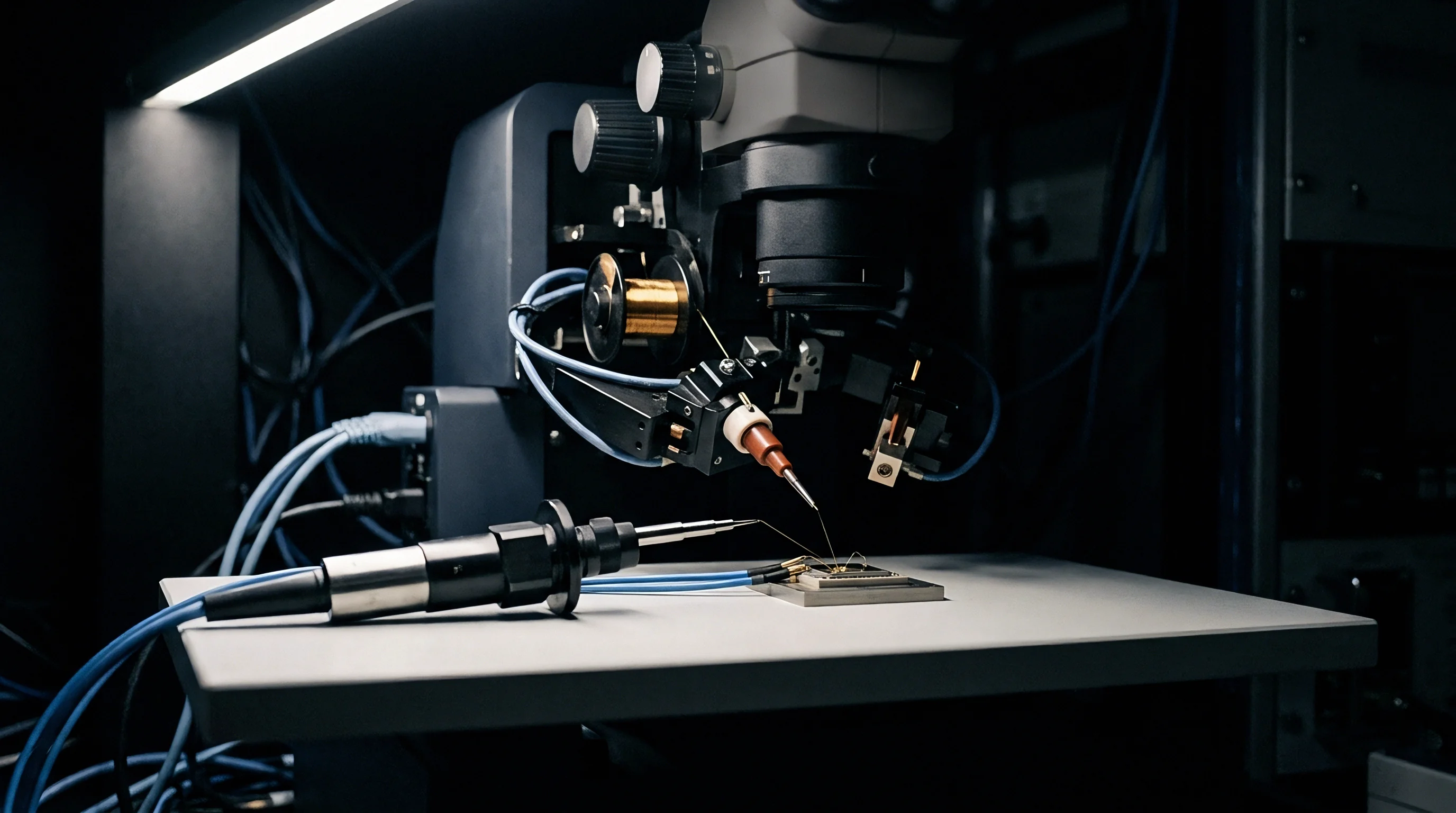
Pin tip topography is quantified by root-mean-square roughness Rq and arithmetic mean deviation Ra. Machining marks, chemical etching artifacts, and electroplating nodules create surface profiles with spatial wavelengths ranging from 100 nanometers to 5 micrometers. When two rough surfaces come together under normal contact force, initial contact occurs solely at the highest summits.
Elastic deformation governs initial contact. As pin insertion travel increases, local stress exceeds the yield strength of the softer contact finish, inducing plastic flow. The total contact area divides into discrete conduction spots scattered across the mating zone, funneling radio frequency current through narrow constrictions that raise local current density orders of magnitude above nominal pin bulk density.
The relationship between surface roughness metrics and high-frequency contact resistance connects directly to micro-topography geometry:
- Arithmetic Mean Roughness Ra defines the center-line average height variation across the contact tip profile, serving as the baseline quality metric on socket procurement drawings.
- Root Mean Square Roughness Rq heavily weights larger peaks and valleys, correlating with high-frequency surface scattering losses and localized current constriction.
- Peak To Valley Height Rz measures extreme surface excursions that pierce protective thin gold flash coatings, accelerating base metal oxidation and contact resistance drift.
- Mean Asperity Slope Rda dictates the micro-constriction angle where radio frequency current diverts around surface depressions, increasing localized loop inductance.
High local current density causes resistive self-heating at asperity junctions. In high-power test setups ~ such as Wi-Fi 7 power amplifier verification running plus 30 dBm transmit levels ~ asperity temperatures climb rapidly. Localized thermal expansion and material softening alter the mechanical compliance of the contact over repeated device insertions.
Direct-current four-wire resistance under 30 milliohms is often cited to verify contact integrity regardless of surface roughness finish.
Standard machining finishes are often justified on the grounds that DC resistance checks prove mating surface adequacy, despite the severe signal degradation that occurs at higher frequencies.
Skin
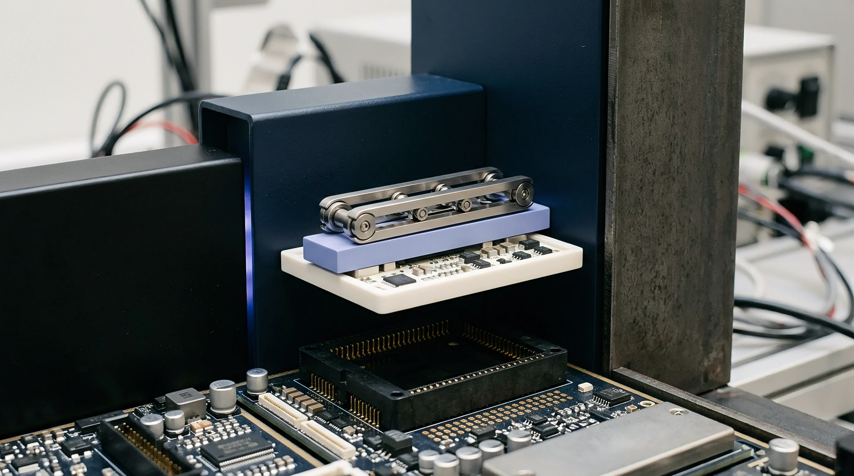
Conduction paths change entirely once signal frequencies drive skin depth below the arithmetic roughness amplitude Ra. At 60 GHz, skin depth in cobalt-hardened gold plating measures 0.32 micrometers. If pin tip Ra measures 0.50 micrometers, electromagnetic energy flows along the convoluted profile of peaks and troughs, increasing the effective conduction path length by 20 to 60 percent compared to an optically smooth boundary.
This surface-following current distribution introduces two distinct loss mechanisms: conductor attenuation increases because of the longer resistive route, while micro-cavities between mating asperities act as parasitic inductive-capacitive networks that disturb the characteristic impedance of the socket channel.
Evaluating a 50-ohm coaxial spring probe designed for 28 GHz automated testing highlights these effects. Table 2 details the modeled and measured high-frequency performance variations across three distinct surface finish grades under identical mechanical preload.
| Surface Finish Grade | Pin Tip Ra (um) | Nominal Preload (gf) | DC Resistance (mOhm) | RF Resistance at 28 GHz (Ohm) | Insertion Loss S21 (dB) | Return Loss S11 (dB) |
|---|---|---|---|---|---|---|
| Diamond Lapped | 0.05 | 25 | 16.2 | 0.48 | -0.12 | -28.5 |
| Precision Micro-Machined | 0.20 | 25 | 17.8 | 0.74 | -0.28 | -22.1 |
| Standard Turned | 0.55 | 25 | 19.5 | 1.36 | -0.65 | -15.3 |
| Degraded / Worn | 1.10 | 25 | 28.4 | 2.85 | -1.42 | -9.8 |
Signal integrity degrades rapidly in the standard turned and degraded finishes. Return loss drops to negative 15.3 dB on the standard turned pin, introducing substantial reflection into the transceiver test fixture. Signal reflections compromise error vector magnitude measurements on modern high-order modulation schemes like 4096-QAM.
Wide roughness variations across multi-pin socket arrays introduce channel-to-channel skew, skewing beamforming calibration algorithms in phased-array radar and 5G test setups.
Surface roughness must remain below half the skin depth to prevent excessive radio frequency insertion loss.
Precision manufacturing techniques maintain consistent surface topography. Chemical mechanical polishing, electropolishing, and diamond-tool turning produce tip geometries with Ra values below 0.08 micrometers. Smooth finishes maintain high-frequency current cohesion, suppressing signal scattering and phase jitter during automated production testing.
Wear
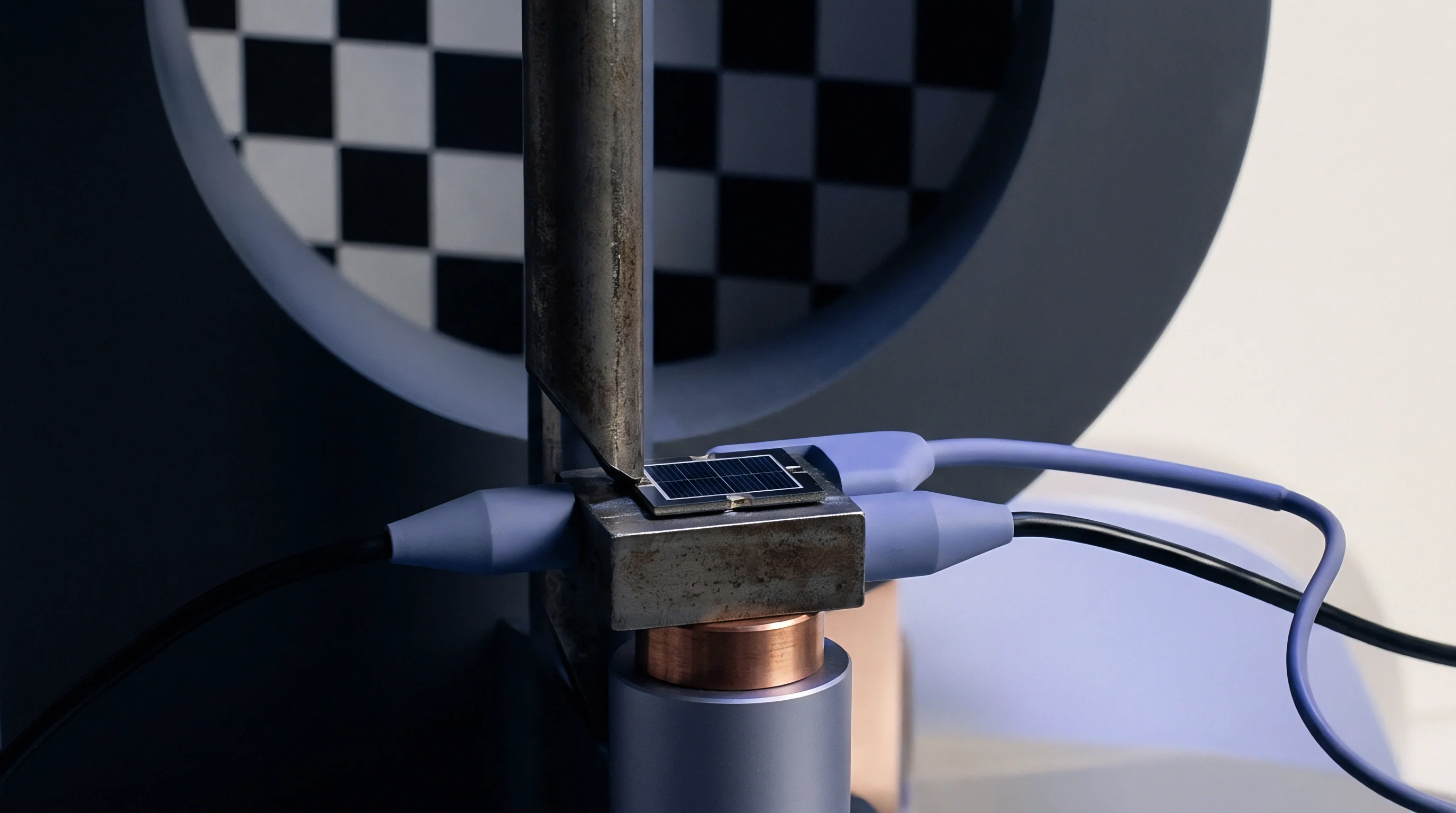
Repetitive cycling in high-volume production test sockets progressively alters contact surface roughness. Automated handlers cycle test sockets through hundreds of thousands of insertions. Device contact pads, typically copper finished with organic solderability preservatives, lead-free solder balls, or electroless nickel immersion gold, interact mechanically with the socket tips through micro-wiping, sliding friction, and cyclic impact.
Abrasive wear strips the protective hard-gold finish over time. Solder particles transfer from device pads to the pin tips through adhesive wear mechanisms. Transferred tin and lead-free alloys form intermetallic compounds with the underlying nickel barrier plate, increasing roughness and building non-conductive oxide layers on asperity peaks.
Test floor managers monitor test socket degradation through specific sequential maintenance actions:
- Initial Contact Verification records baseline four-wire DC resistance, high-frequency S-parameters, and time-domain reflectometry profiles on clean, uncycled contactor pins.
- Periodic S-Parameter Re-Measurement tracks insertion loss degradation and return loss shift at specified insertion milestones under automated test handler operation.
- Surface Profile Topography Scanning quantifies Ra and Rz changes using non-contact optical profilometry when RF performance drifts beyond allowable limits.
- Abrasive Scrub Cleaning Cycles remove accumulated solder debris, oxide flakes, and organic contamination from the contactor tips using specialized cleaning pads.
- Socket Pin Replacement swaps worn pin arrays when base metal exposure or permanent asperity deformation exceeds RF loss tolerances.
Base metal exposure accelerates galvanic corrosion in humid production environments. Nickel and copper migrate to the contact interface, forming passive dielectric films that block direct metallic conduction. Current is forced to tunnel through thin oxide layers or bridge through fewer remaining gold asperities, drastically multiplying micro-constriction resistance.
Per IPC-9502 test guidelines, contactor replacement triggers when RF insertion loss degrades by more than 0.5 dB from initial baseline calibration.
Passive intermodulation distortion emerges as contact surfaces degrade. Non-linear conduction across oxidized asperity interfaces generates spurious mixing products when multi-carrier or full-duplex radio signals traverse the test socket. Receiver sensitivity measurements fail during production screening when intermodulation spurs fall into the receive band of the device under test.
Plating thickness of hard gold over nickel barriers directly alters the rate of surface roughness degradation under extreme multi-cycle mechanical scrubbing.

Allowance
Radio frequency test socket specifications establish mechanical, electrical, and surface topography tolerances. Engineering drawings define acceptable surface roughness alongside plating chemistry, spring force, and geometric co-planarity. Pin manufacturers manage plating bath parameters, pulse-plating current density, and brightener additives to produce dense, low-roughness deposits.
Procurement teams evaluate cost tradeoffs between baseline standard-turned pins and precision-polished alternatives. While precision surface finishing adds unit cost to the test socket assembly, this initial tooling expense is balanced against extended socket lifespan, reduced cleaning downtime, and preserved silicon yield across high-volume production runs.
RF test socket design parameters dictate overall production line stability:
- Normal Contact Force maintains adequate plastic deformation of asperities to guarantee stable a-spot contact while preventing device pad puncture.
- Plating Hardness Rating specifies Knoop or Vickers hardness of gold and alloy coatings, controlling the rate of mechanical wear and surface gouging.
- Underlayer Barrier Integrity ensures continuous nickel deposition without pinholes, preventing copper substrate migration to the outer contact boundary.
- Tip Geometry Profile concentrates mechanical force at specific wiping edges to clear surface oxides during device touchdown without generating abrasive burrs.
Production facilities establish strict socket replacement intervals based on RF contact resistance budgets. Test sockets designated for millimeter-wave operation enforce tighter Ra allowances than low-frequency sockets. Automated test fixtures run continuous yield monitoring algorithms that correlate device test failures with specific socket contact positions, isolating roughness-induced measurement drift before lot-level scrap occurs.
Contact resistance across high-frequency test sockets remains an active design variable governed by surface roughness, material properties, and operational frequency. Managing micro-topography ensures repeatable RF test performance, accurate device characterization, and reliable high-volume semiconductor manufacturing.