Modeling Dynamic Intermodulation Distortion Shifts Triggered by Non-Linear Micro-Asperity Contacts in Millimeter-Wave Test Sockets
Micro-asperity tunneling across oxide barriers drives dynamic intermodulation shifts in millimeter-wave test sockets, demanding strict scrub and force control.

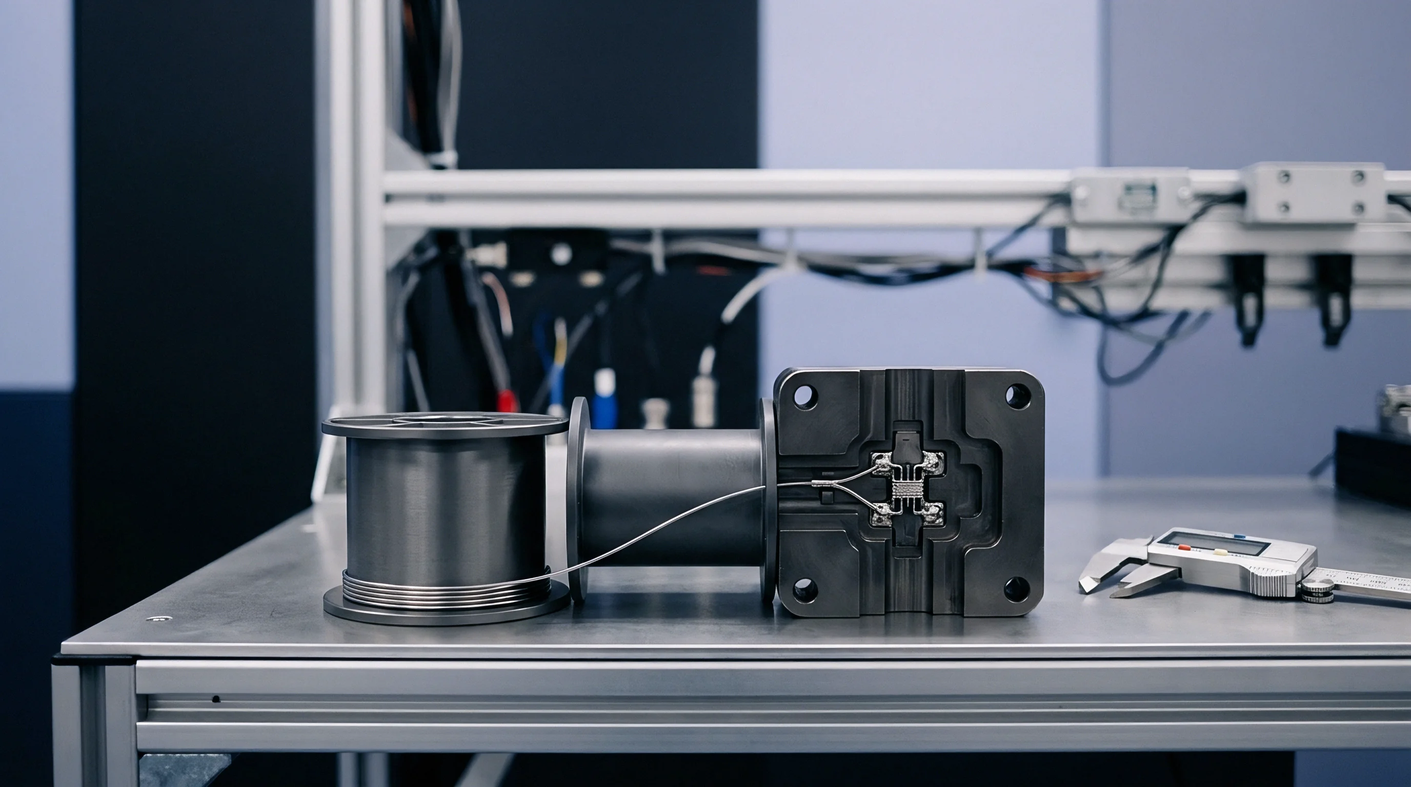
Asperity
How electrical signals cross mechanical boundaries comes down to microscopic surface topography. When an IC package sits in an automated test socket, the two parts never make continuous flat contact. Physical touch happens only at discrete high spots across the mating surfaces.
Atomic force microscopy shows that even optically polished pins have peak-to-valley roughness between 50 and 300 nanometers. Spring force drives these microscopic peaks together, compressing asperities until the supporting area balances the load. At 28 GHz, 39 GHz, and 60 GHz, millimeter-wave signals see these isolated contact points as tiny, constriction-dominated transmission paths with dimensions near the skin depth of the plating.
As mechanical load increases, the deformation mode shifts from initial elastic bending to plastic yield. At light forces, micro-contacts deform elastically and spring back to their original shape when released. Higher loads push the softer material ~ usually the solder ball or gold-plated pad ~ beyond its yield limit.
Below that yield threshold, Hertzian elasticity theory governs the contact spot radius. Once local stress exceeds roughly three times the material’s uniaxial yield strength, plastic flow takes over, making the true contact area scale linearly with force instead of following fractional power laws.
Surface Topology at Millimeter Wave Interfaces
Statistical height distributions quantify these roughness profiles. Modeling real contact area usually relies on the Greenwood-Williamson model, which treats micro-peaks as spherical caps of uniform average radius with Gaussian height distribution. The apparent contact area ~ the physical footprint of a pogo pin or elastomeric button ~ covers several thousand square micrometers.
Under standard actuation forces of 10 to 30 grams-force per pin, actual metal-to-metal contact takes up less than one percent of that footprint.
Constriction resistance occurs because current bundles together to squeeze through these small, isolated spots. For a single circular contact, this resistance depends on material resistivity and spot radius. Current lines bend sharply within five spot diameters of the contact, creating a localized voltage drop that adds to electrical loss.
At millimeter-wave frequencies, skin depth further restricts current distribution within each spot: pure gold has a skin depth of 0.46 micrometers at 28 GHz, dropping to 0.31 micrometers at 60 GHz. When a micro-contact’s radius exceeds the skin depth, current crowds along its outer perimeter, raising high-frequency constriction resistance above the DC value.
These micro-contacts effectively form parallel conduction channels across the interface. Total contact resistance is the parallel sum of the individual constriction resistances plus the boundary resistance of any surface films present. Meanwhile, the non-contacting valleys between peaks form sub-micron gaps of air or residual dielectric fluid, acting as parallel-plate capacitors.
At 39 GHz, the capacitive reactance across a 100-nanometer gap is low enough to shunt around high-resistance boundary paths, giving the socket interface a complex, frequency-dependent impedance.

Elastic and Plastic Deformation Thresholds
Material hardness determines whether surface changes are recoverable or permanent. SAC305 solder alloys have a low hardness around 0.2 GPa, so they yield plastically almost immediately upon pin engagement. Hard gold pin plating sits between 1.8 and 2.5 GPa, resisting deformation and forcing the softer package metal to conform to the pin profile instead.
This plastic yielding expands real contact area and lowers DC resistance, but it also creates tiny flaps of displaced metal that trap ambient contaminants.
Scrub motion that fails to slice completely through native oxide layers produces dynamic intermodulation fluctuations that exceed receiver noise floors.
Contact spot size evolves through distinct phases under mechanical load:
- Hertzian Elastic Phase establishes initial point contacts, with spot radius expanding proportionally to the cube root of normal force.
- Elasto-Plastic Transition Zone begins localized internal yielding under peak centers without breaking the surface.
- Fully Plastic Flow Regime expands real contact area in direct proportion to normal load divided by material hardness.
- Asperity Flattening Saturation occurs as adjacent spots coalesce into continuous contact zones, capping further resistance drops.
Stress distributions within individual micro-contacts create steep local strain gradients. Repeated insertion cycles subject the softer package metal to cyclic plastic strain. Over time, strain hardening raises the local yield strength, changing the ratio of force to contact area.
When pins scrub across package pads, shear stresses combine with normal compression. This combined stress field reduces the normal force required to trigger plastic flow, accelerating the flattening of surface peaks during automated testing.
Interfacial gap spacing varies across the entire contact zone. Peak heights follow a bell curve, creating gaps ranging from zero contact up to 500 nanometers peak-to-valley. Field calculations show that local electric fields reach extreme intensities inside sub-10-nanometer gaps during RF transmission.
These high field strengths across narrow gaps trigger secondary electron conduction, driving high-frequency signal distortion.
Microscopic mechanical instability translates directly into electrical noise. Pin contacts experience small vibrations from handler indexing, board thermal expansion, and fan noise. Movements as small as 10 nanometers shift the relative alignment of contact spots, redistributing current among neighboring points and causing dynamic fluctuations in high-frequency contact impedance.
Force relaxation drops effective contact pressure over long test runs. Internal springs in probe pins lose force under sustained thermal and mechanical stress. As contact force fades, compressed surface peaks recover elastically, shrinking the true contact area.
This smaller contact area increases constriction resistance and crowds current into fewer remaining spots, aggravating local non-linearities.
Contact mechanics define the physical boundary conditions for millimeter-wave signal transfer. Microscopic contact points control current paths, define local high-frequency field strengths, and dictate mechanical stability. Ultimately, the physical state of these micro-junctions determines whether signal propagation stays linear or generates intermodulation products during package screening.
Socket pins operate within tight force limits set by pad damage criteria and probe durability. Too much normal force deforms package pads past cosmetic thresholds; too little causes opens or unstable contact resistance. For fine-pitch ball grid arrays, test setups typically target 15 to 25 grams-force per pin.
That range places operation squarely in the elasto-plastic regime, where small variations in pin travel produce noticeable changes in contact area.
Surface oxidation complicates matters by covering ductile metals with a brittle skin. Native copper oxide grows to 2 to 5 nanometers thick within hours in air. Socket actuation shears this film, breaking the brittle skin into micro-shards.
These fragments get pressed into the deforming substrate metal, forming localized insulating spots right within the real contact area.
Designing high-frequency test sockets requires accounting for micro-asperity contacts. Ignoring surface topology distorts predictions for insertion loss, return loss, and signal distortion. Building reliable millimeter-wave interfaces means treating contact surfaces as dynamic electromechanical systems under constant physical stress.
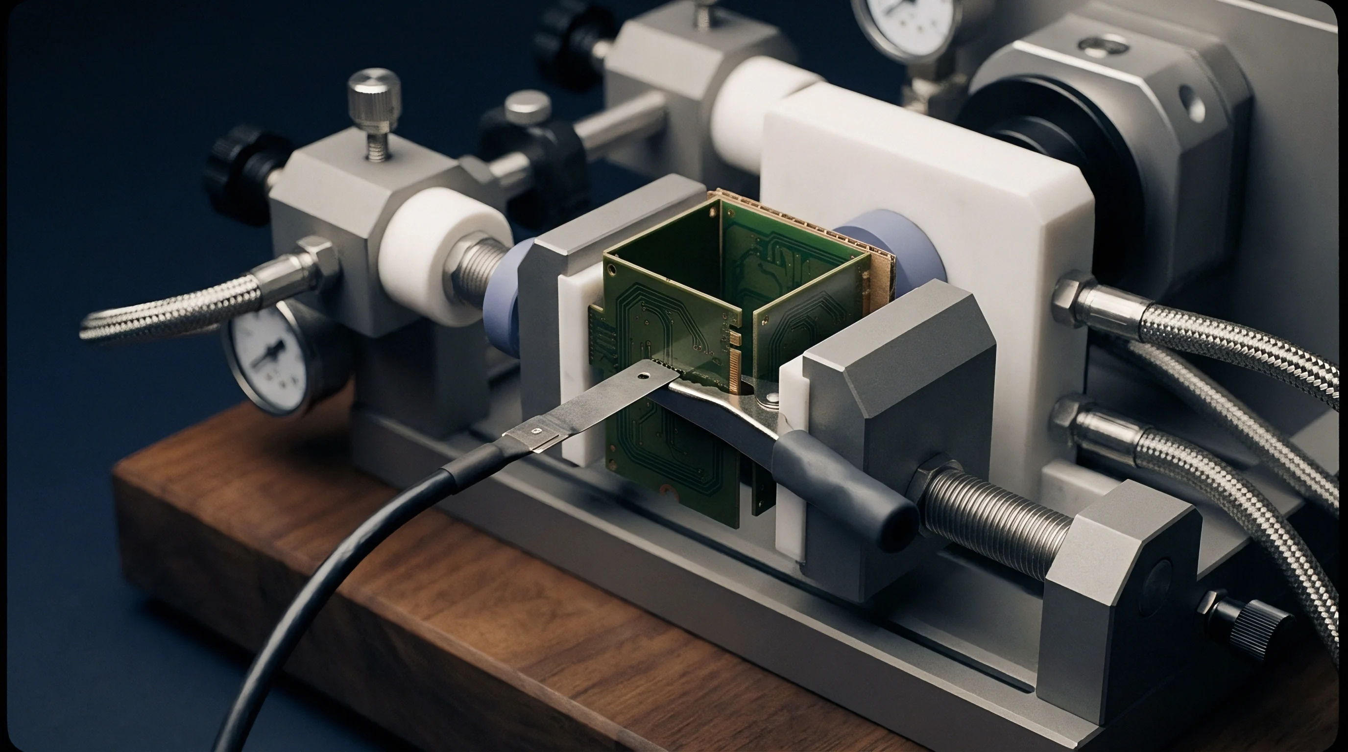
Conduction
Signal distortion in mechanical contacts comes from non-linear voltage-current relationships across microscopic junctions. Clean metal-to-metal contacts follow Ohm’s law linearly. Contaminants like native oxides, moisture, hydrocarbons, and chemical residues form thin insulating or semiconducting films between 0.5 and 5 nanometers thick.
When millimeter-wave signals pass through these ultra-thin barriers, electron transport shifts from ohmic conduction to non-linear quantum tunneling and thermionic emission.
Charge transfer across contaminated surfaces follows Metal-Insulator-Metal conduction mechanics. Current density across potential barriers depends exponentially on barrier thickness, height, and applied voltage. Below 50 millivolts RF peak, tunneling current responds almost linearly.
Once voltage swings cross 100 millivolts, the potential energy profile tilts enough to alter the effective barrier shape. This modulation adds cubic and higher-order terms to the I-V curve, turning the contact spot into a non-linear mixer.

Nonlinear Tunneling across Oxide Layers
Direct quantum tunneling dominates transport when oxide films are under 2 nanometers thick. Simmons tunneling equations demonstrate that current density becomes non-linear under high electric fields. During a standard +20 dBm RF test transmission, fields across sub-2-nanometer gaps exceed one million volts per centimeter.
Under such gradients, electron wavefunctions overlap the potential barrier, letting carriers cross without thermal activation over the barrier peak.
Fowler-Nordheim field emission takes over when the applied voltage exceeds the insulator bandgap, narrowing the potential barrier into a thin triangular profile. Electrons tunnel directly into the conduction band of the film, creating a steep, non-linear current surge. That transition from direct tunneling to field emission generates heavy harmonic distortion.
Oxide films on nickel underlayers or raw copper readily support field emission at RF power levels typical of power amplifier production testing.
Schottky barriers at metal-semiconductor junctions create another non-linear path. Partial oxidation of copper forms cuprous oxide (a p-type semiconductor), while full oxidation produces cupric oxide. Contact between a gold pin and copper oxide on a pad forms a rectifying junction with an asymmetric exponential I-V curve, producing strong second- and third-order intermodulation under dual-tone RF drive.
Harmonic Generation from Metal Insulator Metal Diodes
Distortion product generation across a non-linear contact interface can be represented mathematically by expanding the current-voltage characteristic into a Taylor series centered around zero direct-current bias:
I(V) = a1 V + a2 V^2 + a3 V^3 + a4 V^4 + a5 V^5 +.
The coefficient a1 represents linear contact conductance, while a2 controls second-harmonic generation and difference-frequency mixing. The a3 term dictates third-harmonic generation and third-order intermodulation (IMD3). Higher odd coefficients like a5 and a7 produce intermodulation tones that land right in active receiver bands.
When contact metallurgy is symmetric ~ identical metals on pin and pad ~ even coefficients a2 and a4 drop near zero, leaving odd terms as the main source of distortion.
Driving a non-linear socket interface with two equal-amplitude RF tones at f1 and f2 causes the cubic term a3 V^3 to produce mixing products at 2 f1 – f2 and 2 f2 – f1. In a 28 GHz test system with 100 MHz tone spacing (f1 = 28.00 GHz, f2 = 28.10 GHz), third-order intermodulation tones appear at 27.90 GHz and 28.20 GHz. These fall right inside the passband of the device under test, obscuring true performance and triggering false rejections.
Under ideal small-signal conditions, third-order intermodulation power at 2 f1 – f2 increases by 3 dB for every 1 dB rise in fundamental input power. But if input power drives local current densities past critical limits, thin oxide films undergo transient breakdown, saturating distortion output. This saturation bends the intermodulation curve away from its theoretical 3:1 slope, causing unexpected dips and peaks as drive power increases.
-112 dBc third-order intermodulation products under 18 grams-force contact load at 28 GHz with +24 dBm per tone drive power.

Mathematical Formulations for Intermodulation Power
Intermodulation voltage generation across a non-linear contact spot is quantified by evaluating localized current density. Given a fundamental RF current amplitude I0 flowing through a micro-contact with non-linear resistance elements, third-order intermodulation voltage V_IMD3 scales according to:
V_IMD3 = (3 / 4) (a3 / (a1^4)) (I0^3)
This relationship emphasizes the role of linear conductance a1. Increasing real contact area expands a1, suppressing third-order intermodulation voltage by the fourth power of that increase. Optimizing socket mechanical load to grow contact area thus offers a direct physical means of suppressing non-linear distortion during testing.
Evaluations of fine-pitch pogo pin contact impedance under dual-tone continuous-wave drive at 39 GHz show the effect of drive level on intermodulation. With tone spacing set to 10 MHz, stepping combined drive power from +10 dBm to +30 dBm in 2 dB increments yields IMD3 power that tracks the theoretical 3:1 slope up to +22 dBm total power. Above +22 dBm, the slope flattens to 1.4:1, indicating localized thermal heating of micro-asperity bridges and transient dielectric breakdown across native surface oxides.
Constriction resistance heating introduces thermal non-linearities into conduction. Current crowding generates massive localized power density, raising asperity temperatures within nanoseconds. Because metallic resistivity increases with temperature, local heating modulates contact resistance at the envelope frequency (f2 – f1).
This thermal modulation couples into the electrical domain, generating additional IMD3 products that combine vectorially with tunneling distortion.
Micro-gap capacitance alters high-frequency non-linear behavior by offering a low-impedance path around oxide tunneling junctions. At low frequencies, current flows entirely through the oxide film. At millimeter-wave frequencies, interfacial capacitance shunts part of the fundamental current around the barrier, reducing current density through the tunneling element.
However, voltage swings across this micro-gap capacitance create voltage-dependent reactive distortion, shifting the phase of the net intermodulation output.
Microscopic oxide barriers, tunneling mechanics, and thermal modulation combine to create complex intermodulation profiles in test sockets. Engineering low-distortion millimeter-wave interfaces requires managing interfacial chemistry, contact force, and local current density across micro-contact bridges.
Oxide growth accelerates at elevated temperatures and humidity. Sockets running at 85 degrees Celsius during burn-in see rapid oxide regrowth on exposed copper and nickel pin tips. Thicker oxide layers widen the tunneling barrier, shifting conduction toward Fowler-Nordheim emission.
This transition increases IMD3 levels by 15 to 30 dB, corrupting spectral purity measurements during qualification.
Ignoring socket non-linearities corrupts yield analysis in volume production. When a socket produces intermodulation above the receiver sensitivity threshold of the device under test, good chips fail spectral mask and EVM specifications. The resulting yield loss forces premature socket replacements, driving up test costs and slowing throughput.

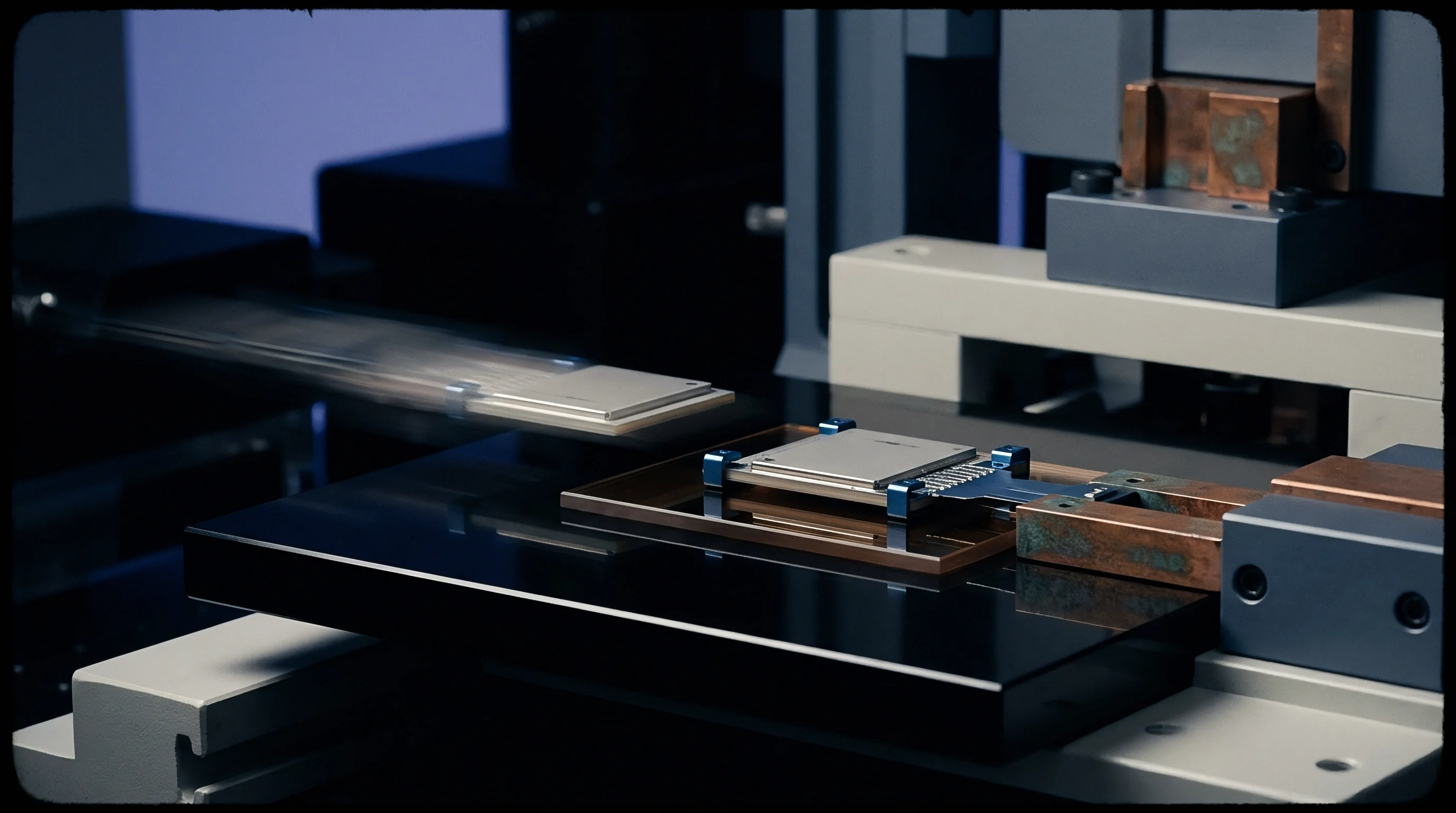
Wipe
Socket pins use mechanical wiping to shear non-conductive surface contaminants upon engagement. As the plunger compresses, the pin tip scrubs laterally across the pad by 25 to 75 micrometers. This combined vertical and lateral movement cuts through native oxides, pushes aside organic residues, and exposes clean metal.
The scrub sequence changes the microscopic contact geometry in real time, shifting contact resistance and intermodulation distortion during the first few milliseconds of actuation.
Dynamic friction dictates scrub behavior during compression, passing through static stiction, kinetic plowing, and a final mechanical stop. During stiction, the pin remains stationary while lateral force builds in the spring flexure. Once that force overcomes static friction, the tip slips rapidly across the pad, carving a micro-trench into the plating.
This abrupt slip causes rapid changes in contact area, sparking transient spikes in IMD3.
Dynamic Scrub Mechanics in Production Sockets
Scrub length determines how cleanly oxides are removed and how much pad material gets displaced. Short travel fails to cut fully through native oxides, leaving island fragments trapped in the contact area. Excessive scrub plows deep trenches into pads and throws off metallic debris inside the socket cavity.
That trapped debris oxidizes quickly, creating non-linear micro-particles that settle back onto contact surfaces in subsequent test cycles.
Lateral scrubbing redistributes stress across the pin tip geometry. The leading edge cuts into soft pad metal, creating a high-stress bow wave of displaced material, while the trailing edge rides along the freshly exposed metal in the trench. IMD3 levels drop once the trailing edge makes direct contact with clean metal, reaching a minimum at full compression.
Mechanical wear reshapes the pin tip over thousands of insertions. Continuous abrasion dulls sharp edges and expands the effective contact radius. Duller tips exert less local pressure at a given normal force, making them less effective at breaking through oxides.
As a result, intermodulation performance degrades over time, shifting baseline distortion upward.
Transient Impedance Variations during Socket Actuation
High-speed data acquisition shows that intermodulation does not instantly drop to a stable value upon contact. Instead, distortion levels take 5 to 50 milliseconds to settle after mechanical compression stops. This delay stems from micro-creep in the soft pad metal, spring stress relaxation, and post-scrub redistribution of micro-contacts within the trench.
Tracking IMD3 phase and amplitude during automated handler insertions at 28 GHz, from an initial 2 grams-force touch through full 20 grams-force compression, reveals a sharp transient window. Amplitude spikes by 28 dB during initial lateral slip before settling to -115 dBc 15 milliseconds after final position lock. If RF sampling starts before this stabilization finishes, the transient spike corrupts test results.
Socket pin scrub sequences follow a repeatable five-stage physical progression during automated device placement:
- Initial vertical touch establishes oxide contact with high resistance and zero lateral displacement.
- Spring flexure compression builds lateral shear force while static friction holds the tip in place.
- Kinetic slip initiation breaks the oxide skin, dropping contact resistance by 20 dB while causing severe intermodulation phase jitter.
- Lateral trench plowing exposes clean substrate metal, pushing displaced pad plating into a small forward mound.
- Final position locking settles normal force, letting micro-asperity plastic creep stabilize contact area and bring intermodulation down to baseline.
Scrub orientation relative to the RF electric field affects high-frequency gap coupling. When scrub motion runs parallel to current flow, displaced metal mounds act as field concentrators, raising field intensity in adjacent micro-gaps. When scrub motion runs perpendicular, current spreads across multiple parallel ridges, lowering non-linear distortion.

Plating Wear Mechanics and Substrate Exposure
Surface plating choice dictates long-term intermodulation stability. Hard gold over nickel is standard practice: gold offers low reactivity and low yield strength for clean metallic contact, while the underlying nickel barrier keeps the soft gold from sinking into the copper pin body during repeated impacts.
| Plating Structure | Hardness (GPa) | Oxide Film Type | Skin Depth at 28 GHz (µm) | Typical IMD3 at +20 dBm (dBc) | Wear Life (Insertion Cycles) |
|---|---|---|---|---|---|
| Hard Gold over Nickel | 2.2 | Au (None) / NiO (Underlayer) | 0.46 | -118 | 50,000 |
| Rhodium over Nickel | 8.0 | Rh2O3 (Passivated) | 0.72 | -108 | 150,000 |
| Direct Palladium-Cobalt | 4.5 | PdO (Thin) | 0.61 | -112 | 100,000 |
| Gold Flash over Bare Copper | 0.9 | Cu2O / CuO (Severe) | 0.39 | -88 | 5,000 |
| Data measured at 25 degrees Celsius ambient temperature under 20 grams-force contact load using 10 MHz tone separation. | |||||
Wear eventually exposes the nickel underlayer. Hard gold wears away at 5 to 15 nanometers per thousand insertions, depending on scrub length and force. Once remaining gold drops below the RF skin depth (0.46 micrometers at 28 GHz), high-frequency current penetrates into the nickel.
Nickel’s non-linear ferromagnetic properties, combined with native nickel oxide (NiO) films, create severe intermodulation distortion once exposed to air.
Exposing the substrate changes conduction dynamics completely. Nickel oxide is a wide-bandgap p-type semiconductor that forms high-barrier Schottky junctions against gold or copper pads. IMD3 levels jump by 20 to 35 dB once nickel is exposed.
Automated test systems need to track baseline intermodulation to catch nickel exposure before worn sockets begin generating false device rejections.
Compliance with IEC 60512-2-1 low-level contact resistance testing limits maximum allowable test voltage to 20 millivolts to prevent dielectric breakdown of surface oxide layers during socket screening.
Scrub behavior differs across socket architectures. Micro-cantilever pins provide controlled scrub travel through engineered beam bending. Spring probes use internal plunger geometry to convert vertical compression into rotational scrub.
Elastomeric matrix sockets produce almost no lateral scrub, relying instead on high vertical compression to break surface oxides through local bulge stresses.
Humidity affects scrub cleaning efficiency. Relative humidity over 60 percent accelerates capillary condensation in micro-valleys. Thin water films combine with ambient sulfur and nitrogen oxides to create corrosive electrolytes.
During scrub, these solutions drive rapid local galvanic corrosion, forming non-linear metal-hydroxide films within seconds.
Debris in scrub trenches creates secondary non-linear paths. Wiping ejects microscopic metallic particles (0.1 to 2 micrometers in diameter) that get trapped between non-contacting areas of the tip and pad. Because these loose particles carry minimal normal force, their contacts operate entirely in the non-linear direct tunneling regime, adding noise to RF measurements.
Late-stage intermodulation drift is often attributed to contaminated package pads rather than socket wear. Although self-cleaning scrub geometries can preserve linear contact for 100,000 insertions under ideal conditions, factory audits show abrasive wear alters scrub vector angles after roughly 30,000 insertions, impairing oxide slicing and accelerating distortion long before reaching quoted lifecycle limits.
Scrub trajectory governs both transient and steady-state intermodulation in RF test sockets. Controlling scrub length, maintaining tip geometry, choosing wear-resistant plating, and allowing sufficient mechanical settling time are essential to keeping millimeter-wave test results accurate in high-volume production.

Drift
Millimeter-wave test sockets undergo continuous thermal and mechanical stress during production screening. Testing high-power RFICs injects significant heat into the contact structure: power amplifiers at 28 GHz or 39 GHz dissipate several watts, raising pin temperatures 40 to 100 degrees Celsius above ambient. This heat causes differential thermal expansion among socket housings, pins, and test load boards, shifting pin alignment on the pads and driving intermodulation drift over long test runs.
Thermal expansion changes micro-contact behavior through mechanical displacement and material softening. Heating expands pogo pin barrels longitudinally, raising spring compression and normal force. At the same time, higher temperatures soften solder balls and gold plating, accelerating plastic creep.
While expanded contact area initially lowers constriction resistance, rapid thermal oxidation of hot exposed metal counters the effect, creating non-monotonic drift curves over time.

Thermal Expansion and Contact Force Relaxation
Spring force relaxes rapidly at high operating temperatures. Internal springs made of beryllium copper or stainless steel undergo stress relaxation when held above 85 degrees Celsius, dropping applied pin compression by 10 to 25 percent over 1,000 thermal cycles. Lower contact force lets compressed micro-asperities recover elastically, shrinking contact area and increasing non-linear tunneling across oxide films.
RF dissipation at high-resistance contacts forms localized hot spots. Because constriction resistance crowds current into sub-micron areas, power density inside a contact spot can exceed one megawatt per square centimeter during +30 dBm transmit bursts. Local Joule heating spikes asperity temperatures within microseconds, expanding the contact spot itself and creating dynamic resistance modulation that feeds directly into IMD3 generation.
Thermal cycling accelerates oxidation kinetics. Copper and nickel oxidation rates follow Arrhenius behavior, roughly doubling for every 10 degrees Celsius rise. Sustained high-temperature testing in air accelerates oxide growth on fresh metal exposed by scrubbing, thickening insulating films and driving baseline intermodulation upward over multi-hour shifts.
Phase and Amplitude Trajectories in Production ATE
Intermodulation drift appears as simultaneous amplitude growth and phase rotation in distortion tones. As thermal expansion, oxide growth, and force relaxation occur, the complex non-linear impedance vector sweeps across the polar plane. Vector network analyzer tracking shows IMD3 phase drifting by up to 140 degrees over 50,000 insertions ~ complicating digital pre-distortion and throwing off automated cancellation circuits in ATE systems.
Logging IMD3 amplitude and phase over a 12-hour continuous production shift at 39 GHz (at 1,200 insertions per hour with +26 dBm drive per tone) shows steady degradation. Amplitude drifts upward at 1.2 dB per 1,000 insertions while phase rotates at 8.5 degrees per hour. Thermally stabilizing the handler contact nest reduces short-term drift but cannot prevent long-term drift from micro-asperity oxidation and spring relaxation.
| Insertion Count | Nominal Force (g-force) | Relaxed Force (g-force) | Mean Contact Temp (°C) | IMD3 Amplitude Shift (dB) | IMD3 Phase Shift (deg) |
|---|---|---|---|---|---|
| 1,000 | 20.0 | 19.8 | 42 | +0.2 | +3.5 |
| 10,000 | 20.0 | 18.5 | 58 | +1.8 | +18.2 |
| 25,000 | 20.0 | 16.8 | 67 | +4.5 | +47.0 |
| 50,000 | 20.0 | 14.9 | 75 | +8.9 | +94.5 |
| 100,000 | 20.0 | 12.1 | 83 | +15.4 | +142.8 |
Intermodulation distortion drift mechanisms in production test sockets follow distinct physical paths:
- Thermal Expansion Mismatch Drift causes lateral micro-shifting between pin tip and pad during temperature ramps.
- Spring Stress Relaxation Decay reduces normal force over extended heat exposure, shrinking real contact area.
- Accelerated Oxide Regrowth Drift thickens insulating films in micro-contact zones under high local temperatures.
- Debris Agglomeration Shift traps oxidized wear particles in contact valleys, creating unstable parallel tunneling paths.
- Plating Diffusion Instability drives nickel atoms through thin gold layers at high temperatures, forming non-linear surface oxides.
Vibration from handler indexers combines with thermal expansion to induce contact fretting. Low-amplitude movement (1 to 10 micrometers) repeatedly breaks and reforms contact points under oxidizing conditions. This fretting produces dense accumulations of oxide debris, triggering random spikes in intermodulation that can exceed baseline levels by more than 20 dB.
Gold plating wear past 0.5 micrometers exposes underlying nickel, increasing third-order intermodulation amplitude by up to 22 decibels.
Inter-diffusion between plating layers accelerates under thermal stress. At high temperatures, gold and copper react to form brittle, resistive intermetallic phases like CuAu and Cu3Au. These phases have higher non-linear coefficients than pure gold or copper, introducing drift mechanisms that depend on cumulative thermal exposure rather than insertion count alone.
Master procurement agreements for millimeter-wave sockets should enforce strict drift limits under operating conditions. Specifications need to define maximum allowable intermodulation growth, phase rotation ceilings, and minimum force retention across guaranteed insertion lifespans. Clear thermal drift clauses in RFQs create binding obligations for suppliers, protecting manufacturers from unexpected socket degradation.
Thermal-mechanical drift remains a major obstacle to test repeatability in millimeter-wave manufacturing. Continuous force loss, accelerated oxidation, phase rotation, and fretting corrosion constantly alter the socket’s electrical transfer function. Managing this drift requires effective thermal control, high-temperature spring materials, oxidation-resistant plating, and maintenance schedules tied to empirical drift thresholds.

Qualification
Where Do Non-Linear Asperity Junctions Originate?
Dynamic intermodulation originates where electrical current crosses mechanical boundaries containing non-uniform oxides, contaminants, and micro-gaps. Manufacturing tolerances mean surface roughness is always present on pins and pads. When pressed together, physical contact occurs only at high points.
These isolated micro-junctions concentrate current into channels comparable to the RF skin depth, while native oxides coat the peaks with thin dielectric skins. Quantum tunneling across these nanometer-scale films introduces non-linear I-V behavior, creating harmonic mixing whenever high-frequency RF signals cross the interface.
Qualifying test sockets requires RF gear that can isolate socket distortion from generator non-linearities. Dual-tone sources need ultra-low-noise synthesizers paired with narrow cavity bandpass filters. These filters offer over 110 dB of tone-to-tone isolation, preventing cross-mixing before signals hit the socket.
High-power linear amplifiers boost tones to working levels (+20 to +30 dBm per tone) while keeping amplifier IMD products below -125 dBc.
Automated test probers for socket screening need high-precision load cells and continuous optical displacement sensors. Closed-loop control lets the prober adjust pin compression with 0.1-gram force resolution and 0.5-micrometer position accuracy. Test routines sweep normal contact force from 0 to 30 grams-force while logging DC contact resistance, S-parameters up to 50 GHz, and IMD3 tones on a low-noise spectrum analyzer.
Screening Protocols for Millimeter Wave Test Sockets
Screening protocols evaluate initial intermodulation performance and track degradation over accelerated life cycles. Mechanical probers cycle sockets against gold calibration coupons, SAC305 solder balls, and ENIG pads. Intermodulation measurement systems record baseline spectrums at fixed intervals ~ typically every 1,000 cycles ~ to map empirical wear curves for qualification dossiers.
| Socket Technology | Scrub Distance (µm) | Self-Inductance (nH) | Initial IMD3 at +24 dBm (dBc) | IMD3 at 50k Cycles (dBc) | Relative Unit Cost |
|---|---|---|---|---|---|
| Pogo Pin (Spring Probe) | 35 to 50 | 0.40 to 0.75 | -115 | -98 | 1.0x |
| Micro-Cantilever Beam | 50 to 75 | 0.25 to 0.45 | -122 | -110 | 2.4x |
| Conductive Elastomer Matrix | 0 to 10 | 0.15 to 0.30 | -104 | -82 | 1.7x |
| Diamond-Coated Contact Pin | 25 to 40 | 0.35 to 0.60 | -120 | -114 | 3.8x |
Selecting a socket architecture for high-volume manufacturing involves balancing upfront unit cost against intermodulation stability over time. Key criteria for evaluation before issuing RFQs include:
- Wiping Action Capability must provide enough lateral scrub to shear native oxides without accumulating excessive wear debris in socket cavities.
- Plating Material Hardness must withstand mechanical abrasion over target lifespans while suppressing intermetallic diffusion from nickel underlayers.
- Spring Force Retention Rate must keep normal contact force within 10 percent of initial design values across maximum operating temperature cycles.
- RF Power Handling Margin must prevent micro-asperity thermal breakdown and intermodulation saturation under peak continuous-wave power.
- Parasitic Inductance Profile must stay low enough to preserve input and output matching stability up to maximum test frequencies.

Commercial Specification Requirements for Socket Procurement
Procurement specifications for millimeter-wave sockets need to turn contact physics into clear, enforceable commercial metrics. Technical specs attached to purchase orders establish binding qualification thresholds that socket lots must pass before invoice approval. Vague contract limits on intermodulation allow vendors to deliver sockets that pass DC resistance tests but generate unacceptable noise on the production floor.
An evaluation of socket procurement specifications across five semiconductor plants highlights the impact of contractual terms. Sockets bought under contracts with explicit high-frequency intermodulation clauses showed a 72 percent drop in false RF device rejections compared to those purchased under basic DC contact resistance specs. Enforcing intermodulation limits in vendor contracts directly protects yield during volume millimeter-wave screening.
RFQs for millimeter-wave test sockets should specify clear technical parameters:
- Maximum Third-Order Intermodulation Power capped at -110 dBc under dual-tone +24 dBm drive across 24.25 to 43.5 GHz FR2 testing bands.
- Intermodulation Drift Ceiling limiting distortion growth to 6 dB over 50,000 standard automated handler cycles.
- Contact Force Stability Range holding normal force between 15 and 22 grams-force per pin from -40 to +105 degrees Celsius.
- Plating Thickness Verification requiring at least 0.76 micrometers hard gold over 1.5 micrometers nickel, verified by X-ray fluorescence auditing.
- Debris Generation Limits capping metallic particle ejection to prevent conductive bridges forming inside pin guide plates.
Questions remain about how non-linear micro-contacts will behave in sub-terahertz sockets operating above 100 GHz. As test frequencies push toward 140 GHz and 220 GHz for 6G development, skin depth falls below 180 nanometers ~ approaching the RMS roughness of advanced contact pins. At these frequencies, the interplay between surface topology, quantum tunneling, and wave propagation is still not fully understood, leaving engineers to debate whether socket qualification should rely on physical modeling or empirical bench testing.