Mitigating Temperature Induced Phase Noise in Millimeter Wave Substrates
Thermally stable low-TCDk substrates combined with symmetric layout compensation maintain carrier phase integrity and prevent mmWave regulatory emission failures.


Stack
Thermal transients inside high-frequency printed circuit boards alter the effective dielectric constant of transmission line materials, shifting phase velocity and electrical length along millimeter-wave conductors. As operating frequencies move into the 24 GHz to 100 GHz range, small physical and dielectric changes produce electrical phase shifts that degrade vector signal accuracy, increase local oscillator phase noise, and corrupt beamsteering angles in phased-array antennas. Selecting laminates for high-frequency radio front-ends operating across broad thermal windows involves balancing several competing material properties.
Dielectric Thermal Coefficients at Millimeter Wave Frequencies
Signal propagation along microstrip and conductor-backed coplanar waveguide structures depends directly on substrate permittivity stability across the operating temperature window. The temperature coefficient of dielectric constant, designated as TCDk and expressed in parts per million per degree Celsius (ppm/°C), defines how relative permittivity shifts with temperature. Standard low-cost FR-4 materials display TCDk values exceeding +300 ppm/°C, making them unsuitable for millimeter-wave circuits.
Advanced high-frequency substrates constrain this coefficient through selective polymer chemistry and inorganic filler integration.
When temperature rises, the volume expansion of polymer chains decreases bulk density, reducing polarizable molecules per unit volume and driving substrate permittivity downward. Conversely, filler particles like ceramic powders (silica or titanium dioxide) can exhibit positive thermal dielectric coefficients that offset polymer expansion. Balancing polymer expansion against ceramic filler response yields laminates with near-zero TCDk across industrial operating ranges (-40°C to +85°C).
At seventy-seven gigahertz, a dielectric constant drift of zero point zero zero two per degree Celsius shifts the transmission phase by eight degrees across a ten-centimeter feed trace when ambient temperature rises from twenty to sixty degrees Celsius.
Fluoropolymer and Ceramic Composite Behavior
Hydrocarbon ceramic laminates exhibit linear dielectric response profiles from forty below zero to eighty-five degrees Celsius, avoiding the abrupt crystalline transition observed in traditional polytetrafluoroethylene formulations around twenty degrees Celsius. Pure polytetrafluoroethylene (PTFE) undergoes a phase transition between 19°C and 25°C, where room-temperature crystalline restructuring causes a non-linear step change in dielectric constant of up to 1.5 percent. This step change introduces rapid phase jumps in phase-locked loops and power combiners operating near normal ambient room temperatures.
Woven glass reinforcement inside PTFE laminates introduces anisotropy in thermal expansion. Coefficient of thermal expansion (CTE) along the X and Y axes is constrained by glass fibers to 12 to 18 ppm/°C, while Z-axis thermal expansion in un-filled PTFE can exceed 100 ppm/°C. High Z-axis expansion deforms transmission line cross-sections, alters trace capacitance, and stresses plated through-holes during thermal cycling. Thermoset hydrocarbon resins filled with micro-dispersed ceramic particles provide isotropic thermal expansion profiles closer to copper (17 ppm/°C), maintaining spatial stability and line impedance across environmental variations.
| Material Chemistry | Dielectric Constant (Dk at 28 GHz) | Thermal Coefficient of Dk (ppm/°C) | Loss Tangent (Df at 28 GHz) | Phase Stability Rating |
|---|---|---|---|---|
| Unfilled Woven Glass PTFE | 2.17 | -160 to -220 | 0.0009 | Poor (Non-linear step at 20°C) |
| Ceramic-Filled PTFE Composite | 3.00 | -3 to +10 | 0.0013 | High (Isotropic thermal response) |
| Hydrocarbon Ceramic Laminate | 3.48 | +40 to +50 | 0.0037 | Moderate (Linear progression) |
| Liquid Crystal Polymer (LCP) | 2.90 | -50 to -70 | 0.0025 | Moderate (Thin film stability) |
| Low Temperature Co-fired Ceramic (LTCC) | 5.90 | -10 to +15 | 0.0012 | High (Rigid inorganic matrix) |
Selecting laminate materials with balanced expansion coefficients across all axes preserves transmit signal integrity and prevents phase drift from corrupting local oscillator signals.
Metrology
Accurate verification of thermal phase variation requires specialized test procedures, calibrated instrumentation, and precise environmental control. Measuring small phase shifts at millimeter-wave frequencies under changing ambient temperatures introduces significant measurement uncertainty if test cables, connectors, and chamber interfaces are not isolated from thermal effects.
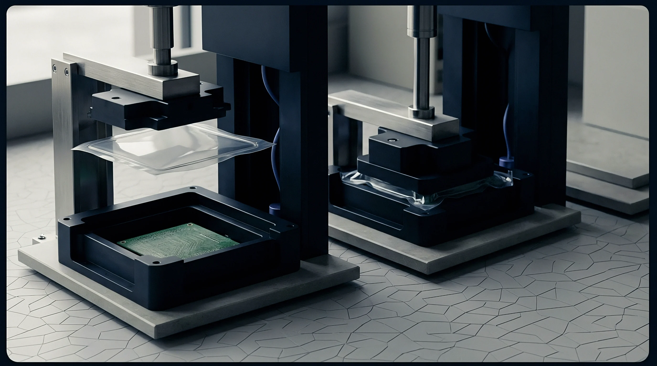
Thermal Chamber RF Characterization Setup
Accurate measurement of temperature-induced phase noise demands continuous vector network analyzer calibration through semi-rigid coaxial cables routed into an environmental test enclosure. Because temperature gradients distort RF signals, test cables passing through chamber walls experience thermal expansion and dielectric phase shifts that can easily exceed the phase shift of the device under test. Phase-stable, thermal-jacketed cables paired with dynamic phase compensation algorithms ensure that observed phase changes originate solely from the device under test.
Vector network analyzer (VNA) calibrations must utilize full two-port short-open-load-thru (SOLT) or line-reflect-line (LRL) standards qualified over the target temperature range. Placing calibration standards inside the chamber during thermal stabilization steps eliminates systemic trace calibration drift. Real-time phase monitoring at millimeter-wave frequencies uses reference signal couplers outside the chamber to establish a phase baseline against thermal noise floors.
Worked Calculation of Phase Noise Degradation
Consider a 39 GHz beamforming array driven by a voltage-controlled oscillator where substrate heating creates a phase shift along the distribution network. A 15-centimeter microstrip line built on a substrate with a thermal dielectric coefficient of -120 ppm/°C operates under a 40°C temperature rise. Phase velocity is defined by:
v_p = c / sqrt(epsilon_r_eff)
For an effective dielectric constant epsilon_r_eff of 2.40 at 25°C, a 40°C rise yields a dielectric change:
delta_epsilon = 2.40 (-120 10^-6) 40 = -0.01152
The updated permittivity becomes 2.38848. Phase delay along the line is given by:
theta = (2 pi f L / c) sqrt(epsilon_r_eff)
At 39 GHz and 25°C, the electrical length across 0.15 meters is:
theta_25 = (2 pi 39 10^9 0.15 / 3.0 10^8) sqrt(2.40) = 18999.64 degrees
At 65°C, the revised electrical length is:
theta_65 = (2 pi 39 10^9 0.15 / 3.0 10^8) sqrt(2.38848) = 18953.97 degrees
The total thermal phase shift equals -45.67 degrees across the 15 cm trace. In a phase-locked loop (PLL) feed network, this rapid phase shift modulates the carrier phase, injecting phase jitter that converts directly into phase noise floor degradation. Assuming a nominal phase noise of -102 dBc/Hz at 100 kHz offset under ambient conditions, uncompensated phase drift of this magnitude degrades the phase noise floor to -94 dBc/Hz at 100 kHz offset, violating standard spectral mask specifications.
The exact contribution of copper surface roughness variations under cyclic heat stress to long-term phase jitter remains unresolved without multi-thousand-hour reliability data.
Attenuation
Signal loss and phase instability interact dynamically inside millimeter-wave dielectrics. As RF energy travels through high-frequency printed structures, dielectric losses convert electromagnetic energy into heat, inducing localized thermal gradients along the transmission path. These self-heating effects compound ambient thermal changes and accelerate phase noise generation.
Can Thermal Phase Shift Drive Radiated Emission Failures?
Carrier signal distortion caused by substrate expansion alters transmitter spectral masks, pushing sideband power past standard regulatory thresholds during temperature chamber sweeps. When temperature variations cause non-uniform phase shifts across array elements, spatial beamforming synthesized in the far field degrades: mainlobe gain drops, sideband grating lobes rise, and sideband spectral energy spills into adjacent frequency bands regulated by standard emission masks.
Transmitters operating under European Telecommunications Standards Institute (ETSI) regulations must comply with occupied bandwidth and out-of-band domain limits across their full declared temperature ranges. A thermal phase shift in the local oscillator distribution network widens phase noise skirts around the fundamental carrier frequency. Widened skirts cause the radio signal to exceed the ETSI EN 305 550 spectral mask, leading to immediate non-compliance during laboratory qualification sweeps.
Loss Tangent Drift and Thermal Dissipation
High dielectric absorption at millimeter wavelengths converts RF energy into heat inside the dielectric matrix, creating local thermal hotspots that compound phase instability. Dissipation factor (tan delta) increases with temperature in most organic laminates. Higher dissipation factors increase attenuation per unit length, generating additional localized thermal energy that exacerbates phase shifts along power amplifiers and transmit lines.
- Dielectric Self-Heating ~ RF attenuation generates localized temperature increases along microstrip lines, driving local permittivity shift independently of ambient surroundings.
- Reciprocal Mixing Expansion ~ Elevated phase noise levels fold nearby off-carrier interference into the receiver baseband, degrading receiver sensitivity metrics under elevated temperatures.
- Beam Pointing Drift ~ Differential phase shifts between array channels alter the relative phase distribution across antenna elements, steering the radiation mainlobe off target.
- Group Delay Distortion ~ Frequency-dependent thermal phase changes introduce unequal signal delays across wideband channels, degrading error vector magnitude (EVM) in digital modulation schemes.
Compliance with ETSI EN 302 217-2 section 5.3 mandates that carrier frequency and phase stability remain within specified boundaries across the full ambient temperature class, or the radio approval certificate is rendered void.
Raw laminate thermal coefficients provided by material vendors do not guarantee final circuit phase performance without accounting for copper etching tolerances or multilayer bonding pressures.

Tolerance
Material manufacturing variances dictate how predictably high-frequency circuits respond to thermal stress. Even when specifying laminates with near-zero nominal TCDk, panel-to-panel and lot-to-lot variances in copper cladding, resin content, and substrate thickness influence total phase shift across temperature ranges.

Copper Foil Cladding and Surface Roughness Impacts
Rolled-annealed metal foils minimize skin effect loss variations across heating cycles compared to electrodeposited alternatives with high surface profiles. At millimeter-wave frequencies, the skin depth of copper drops below 0.4 micrometers at 60 GHz. Rough copper surfaces increase the effective propagation path length for high-frequency currents flowing along the metal-dielectric interface.
As temperature rises, thermal expansion of copper modifies surface profile geometry, altering skin effect losses and effective electrical phase delay.
Electrodeposited copper features tooth-like structures anchored into the dielectric substrate. These profile structures create localized non-uniform electric fields that amplify effective dielectric constant variations under thermal expansion. Specifying ultra-flat rolled copper foils with surface roughness (Rz) below 1.0 micrometer preserves phase stability across thermal cycling and reduces conductor-driven phase jitter.
Manufacturing Control for Batch Phase Consistency
Substrate thickness variations across raw production panels create localized impedance changes that amplify thermal phase shifts in wideband beamforming networks. Controlling resin content distribution during prepreg pressing ensures consistent dielectric performance across multi-layer board builds. Small variations in glass-to-resin ratio across a single panel result in localized thermal expansion differentials, creating phase mismatches between adjacent channels in phased-array transceivers.
| Manufacturing Parameter | Nominal Value | Production Variation Range | Phase Variance per cm (Degrees) | Regulatory Risk Threshold |
|---|---|---|---|---|
| Dielectric Thickness | 100 µm | ± 5.0 µm | 2.4 | High (Impedance shift > 5 Ohms) |
| Copper Roughness (Rz) | 0.8 µm | ± 0.3 µm | 1.1 | Moderate (Attenuation drift) |
| Resin Content Ratio | 45 % | ± 2.5 % | 1.8 | High (TCDk variance shift) |
| Etched Trace Width | 150 µm | ± 7.5 µm | 0.9 | Low (Manageable match drift) |
Selecting materials with tightly controlled dielectric tolerances forms the foundation of thermal noise mitigation. Circuit designers implement specific verification and layout practices during product development:
- Symmetric Feed Architectures ~ Laying out antenna feed lines with identical physical paths balances thermal phase shifts equally across all channels.
- Differential Routing Isolation ~ Routing critical local oscillator paths as differential pairs cancels common-mode thermal phase variations.
- Post-Etching Profile Verification ~ Measuring cross-sectional conductor profiles via optical metrology confirms that trace geometry matches RF model assumptions.
- Material Lot Qualification ~ Conducting sample thermal phase sweeps on incoming laminate batches catches substrate TCDk anomalies before board fabrication.
Specifying microstrip trace geometry compensation based on raw material sheets without verifying post-etching copper thickness leads to uncorrected thermal phase drift during final qualification tests.
Neglecting panel-level thermal dielectric variation during initial board layout forces costly antenna array redesigns and adds months to international regulatory approval timelines.

Certification
Regulatory compliance demands that millimeter-wave radio equipment maintain frequency stability, transmit phase noise profiles, and occupied bandwidth limits under severe temperature stress. Testing occurs inside climate-controlled chambers, where devices undergo multi-hour operational sweeps across declared operating bounds.
Regulatory Test Scenarios across Temperature Extremes
Standard approval testing under FCC Part 15 subpart C and ETSI EN 305 550 requires transmitter frequency stability and spurious emissions compliance from minus twenty to plus fifty-five degrees Celsius. For outdoor backhaul equipment certified under ETSI EN 302 217, ambient test ranges extend from minus forty to plus fifty-five degrees Celsius. Radio transceivers are allowed a warm-up period inside the chamber before maximum power spectral density and phase noise measurements are recorded.
If unchecked thermal shift alters carrier modulation shapes or elevates sideband phase noise above the regulated envelope, the device fails compliance testing and invalidates equipment grants. Retesting requires scheduling new chamber sessions, modifying circuit board layouts, and re-submitting documentation to telecommunication certification bodies (TCBs).
Filing Arithmetic for Global Radio Approvals
Module integration testing across multiple regional jurisdictions demands pre-calibrated temperature chambers to avoid costly chamber time rebooking and missed launch windows. Because operating accredited test facilities costs between $300 and $600 per hour, laboratory chamber testing costs accumulate rapidly. Failing a thermal emission test midway through a three-day certification campaign incurs lost testing fees and causes submittal delays across target export markets.
Execution of a structured compliance verification procedure ensures target regulatory requirements are met before submitting final documentation:
- Pre-screen completed radio assemblies inside an internal environmental chamber across the full target temperature span (-40°C to +85°C) to map phase shift trends.
- Capture vector signal analyzer spectrum masks and phase noise traces at 10-degree increments after allowing thermal equilibrium stabilization.
- Compare observed sideband emissions and carrier phase jitter against FCC Part 15.255 and ETSI EN 305 550 spectral limits to confirm safety margins.
- Compile calibrated temperature chamber data logs into the formal test report dossier required by designated national approval authorities.
| Jurisdiction & Standard | Test Chamber Hours Required | Sample Units Needed | Average Regulatory Fee (USD) | Market Entry Lead Time (Weeks) |
|---|---|---|---|---|
| United States (FCC Part 15.255) | 24 to 36 | 2 (1 Conducted, 1 Radiated) | $8,500 – $14,000 | 4 – 6 |
| European Union (RED / ETSI EN 305 550) | 32 to 48 | 3 (Full functional samples) | $12,000 – $18,500 | 6 – 8 |
| Japan (MIC / Giteki Article 2-1-19) | 20 to 30 | 2 (Modified with test firmware) | $9,500 – $15,000 | 5 – 7 |
| China (SRRC Type Approval) | 40 to 60 | 4 (In-country laboratory testing) | $16,000 – $24,000 | 10 – 14 |
Purchasing agreements incorporating FCC Part 15.255 temperature stability requirements bind substrate vendors to replacement liability if dielectric drift causes compliance failure during formal laboratory testing.