Mitigating Board Noise Desense in Cellular Hardware Radiators
Mitigating board noise desense requires unbroken ground planes, filtered switching stages, and RF shielding cans to preserve receiver sensitivity margins.
Coupling
Receiver desensitization happens when electromagnetic emissions from internal digital and power circuits leak into the antenna within operational frequency bands. When an integrated cellular antenna picks up switching noise from nearby circuitry, the receiver front-end noise floor rises, lowering the signal-to-interference-plus-noise ratio. A three-decibel drop in receiver sensitivity requires the base station to double its transmit power to hold the same throughput, cutting the operating cell radius by about twenty-five percent in free space.
In compact Internet of Things hardware, where antenna elements sit millimeters from processors, power management ICs, and camera serial interfaces, conductive and radiative coupling paths dump internal noise straight onto the radiating elements.
The near-field reactive zone around small antennas inadvertently gathers parasitic electric and magnetic fields. Sub-gigahertz cellular antennas ~ such as those for LTE Band 12 (700 MHz), Band 13 (700 MHz), Band 20 (800 MHz), and Band 28 (700 MHz) ~ have electrical lengths comparable to the entire printed circuit board, making the board itself part of the radiating system. Unshielded power inductors in buck converters radiate magnetic dipole fields whose flux lines pass through the ground return path, driving RF eddy currents across the board.
These currents flow toward antenna feed points, turning the ground plane into a secondary source of noise.
A three-decibel lift in receiver noise floor halves the physical cell area over which a cellular endpoint holds maximum throughput.
High-speed digital traces behave like electric dipole antennas whenever impedance discontinuities disrupt their reference planes. Differential lines for Display Serial Interface, Mobile Industry Processor Interface Camera Serial Interface, or Universal Serial Bus 3.2 gen 1 generate common-mode noise at these mismatches. The resulting common-mode spikes excite resonant modes across the board.
When the cellular antenna picks up these wideband harmonic skirts, receiver sensitivity degrades relative to baseline specs measured in conductively coupled test chambers.
Failing to suppress these near-field coupling paths degrades performance during carrier field testing, leading to de-certification and rejection by network operators.

Choke
Blocking conductive noise on power and signal lines keeps high-frequency spectral spikes from reaching sensitive RF front-end stages. Fast switching edges in gallium nitride or silicon power MOSFETs create harmonics that extend into mid-band cellular allocations between 1.7 GHz and 2.7 GHz. Placing passive attenuating components in series cuts off these conductive paths before RF energy can couple into chassis ground returns or planar antennas.
Conducted Spectral Attenuation Architecture
Filtering requires targeted impedance along supply rails feeding memory arrays and system-on-chip cores. Standard ceramic decoupling capacitors have self-resonant frequencies set by their equivalent series inductance; above twenty megahertz, a typical 100-nanofarad capacitor becomes inductive and stops suppressing noise within cellular bands. Dedicated RF isolation chokes, ferrite beads, and multi-element low-pass filters provide true resistive loss across target uplink and downlink frequencies.
Choosing a ferrite bead requires checking its behavior under continuous DC bias. Direct current saturates magnetic domains in the ferrite core, dropping its high-frequency impedance ~ a bead rated at six hundred ohms at one gigahertz under zero bias often falls to ninety ohms under an operating current of 1.5 amperes. Designers put specialized RF chokes rated for self-resonance in cellular bands right at the switching regulator output pin, before distribution traces extend into the rest of the board.
Passive components lose noise suppression value when direct bias currents drive internal magnetic cores into saturation.
Common-mode chokes deployed across high-speed differential signal pairs attenuate phase-shifted noise while permitting differential information transfer. The table below presents measured attenuation performance across typical cellular reception bands for suppression components installed on five-volt power delivery rails.
| Component Classification | Impedance at Zero Bias (1 GHz) | Attenuation at 700 MHz | Attenuation at 1.8 GHz | Attenuation at 2.6 GHz | Primary Mechanism |
|---|---|---|---|---|---|
| Standard Ferrite Bead | 600 Ohms | -6 dB | -4 dB | -2 dB | Resistive Loss |
| High-Current SMT Inductor | 120 Ohms | -14 dB | -9 dB | -4 dB | Reactive Reflection |
| Dedicated RF Decoupling Capacitor | 18 Ohms | -22 dB | -28 dB | -18 dB | Shunt to Ground |
| Common-Mode Line Filter | 450 Ohms | -19 dB | -16 dB | -12 dB | Phase Cancellation |
| Pi-Network Filter Assembly | 850 Ohms | -34 dB | -38 dB | -31 dB | Reflective and Dissipative |
Internal spread-spectrum clocking algorithms reduce filtering demands, yet radiated harmonic peaks still persist across narrow receiver channels.
Ground
Chassis reference planes serve as the return half of every printed, inverted-F, and slot antenna in consumer and commercial wireless hardware. Any break in ground continuity forces return currents around cuts, vias, or trace penetrations, forming loop antennas that radiate broadband energy. Keeping a solid, uninterrupted copper reference plane beneath cellular radiators minimizes loop areas and contains common-mode potentials that would otherwise reach cellular matching networks.
Layer Stacking and via Fencing
Multilayer board stackups must balance routing density with RF reference integrity. Running high-speed digital buses on internal stripline layers between solid ground planes traps fringing electric fields inside the dielectric substrate. These bounding planes function as parallel plates, preventing capacitive coupling to antenna elements on the outer layers.
- Interplane stitching vias placed along board edges at intervals under one-twentieth of the guided wavelength suppress cavity resonances that would otherwise radiate off the perimeter into antenna keep-out zones.
- Continuous ground copper directly under high-current switching nodes prevents return loops from taking detours, keeping localized magnetic fields contained.
- Split-plane isolation boundaries preserve galvanic isolation between analog and digital sections without causing return path crossovers that generate common-mode noise.
- Solder-mask removal borders enable direct, continuous electrical contact between metal shielding and the main ground plane along perimeter seams.
Connector cutouts act like slot antennas when high-frequency board noise reaches board edges. A slot in a ground plane becomes an effective magnetic dipole radiator when its length reaches half a wavelength; a five-centimeter slot shows quarter-wave resonance near 1.5 gigahertz, spilling noise directly into GPS L1 (1575.42 MHz) and cellular mid-band channels. Placing grounding fingers and closely spaced ground vias around all mechanical openings preserves boundary shielding across the enclosure.
A seam or slot in conductive copper radiates energy into adjacent antennas whenever its physical length approaches a fractional wavelength of internal switching harmonics.
Traces routed across plane splits immediately radiate noise into nearby antennas.

Margin
Evaluating receiver performance requires measuring Total Isotropic Sensitivity degradation across all active cellular bands. During module testing, conductively measured receiver sensitivity is compared against radiated over-the-air figures in an anechoic chamber. Conductive tests bypass the antenna to isolate silicon capability from platform noise, while radiated tests capture antenna efficiency, mismatch loss, and the desensitization penalty created by board-level emissions.

Quantifying Desensitization and Sensitivity Floor Elevation
Thermal noise floor power inside an active receiver channel establishes the baseline reference. This baseline follows the equation:
P_noise = k T B + NF
Where k is Boltzmann constant (1.38e-23 Joules per Kelvin), T is operating temperature in Kelvin (290 K), B is receiver channel bandwidth in Hertz, and NF is receiver front-end noise figure in decibels. For an LTE channel with a 10 megahertz bandwidth and an integrated transceiver noise figure of 4.5 decibels, the thermal baseline power calculates to:
P_noise = -174 dBm/Hz + 10 log10(10,000,000 Hz) + 4.5 dB
P_noise = -174 dBm/Hz + 70.0 dB-Hz + 4.5 dB = -99.5 dBm
Internal board noise behaves as an additive white Gaussian or phase-locked harmonic interferer arriving at the antenna port with power level P_noise_board. Total effective noise power P_total equals the linear addition of thermal noise and coupled board noise:
P_total = 10 log10( 10^(P_noise / 10) + 10^(P_noise_board / 10) )
Sensitivity degradation equates directly to the increase in total input noise power over thermal baseline. If coupled board noise reaching the cellular antenna port equals -102.5 dBm, linear power addition yields:
P_thermal_linear = 10^(-99.5 / 10) = 1.122e-10 milliwatts
P_board_linear = 10^(-102.5 / 10) = 5.623e-11 milliwatts
P_total_linear = 1.684e-10 milliwatts
P_total = 10 log10(1.684e-10) = -97.74 dBm
Sensitivity degradation equals -97.74 dBm minus -99.5 dBm, representing a 1.76 decibel loss in link budget. To assess full system degradation, Total Isotropic Sensitivity incorporates three-dimensional antenna radiation efficiency across spherical measurement points:
TIS = 1 / ( (1 / (4 pi)) integral( Sensitivity(theta, phi) sin(theta) d_theta d_phi ) )
Under isotropic antenna efficiency of -2.5 decibels, conductively measured sensitivity of -99.5 dBm produces an ideal baseline TIS of -97.0 dBm. Coupled board noise elevates receiver threshold to -97.74 dBm, deteriorating radiated TIS to -95.24 dBm.
| Band Designation | Channel Center | Thermal Base Floor | Measured Board Noise | Desense Penalty | Radiated TIS Result |
|---|---|---|---|---|---|
| LTE Band 12 | 737.5 MHz | -99.5 dBm | -101.2 dBm | 2.24 dB | -94.76 dBm |
| LTE Band 13 | 751.0 MHz | -99.5 dBm | -98.0 dBm | 3.82 dB | -93.18 dBm |
| LTE Band 20 | 806.0 MHz | -99.5 dBm | -105.0 dBm | 1.10 dB | -95.90 dBm |
| LTE Band 3 | 1842.5 MHz | -99.5 dBm | -108.5 dBm | 0.51 dB | -96.49 dBm |
| LTE Band 7 | 2655.0 MHz | -99.5 dBm | -112.0 dBm | 0.24 dB | -96.76 dBm |
Board noise affects lower frequencies far more severely. Because antenna dimensions relative to the ground plane at 750 megahertz increase coupling efficiency, low-band channels pick up more interference, whereas gigahertz bands keep near fields tightly confined. Devices in rural deployments may drop connections early on Band 13 while urban cells running on Band 7 maintain uninterrupted throughput.
Carriers enforce strict over-the-air performance under 3GPP TS 34.114 and CTIA Test Plan requirements. Hardware modules that fail to meet specified Total Isotropic Sensitivity limits across required channels cannot obtain carrier certification.
Enclosure
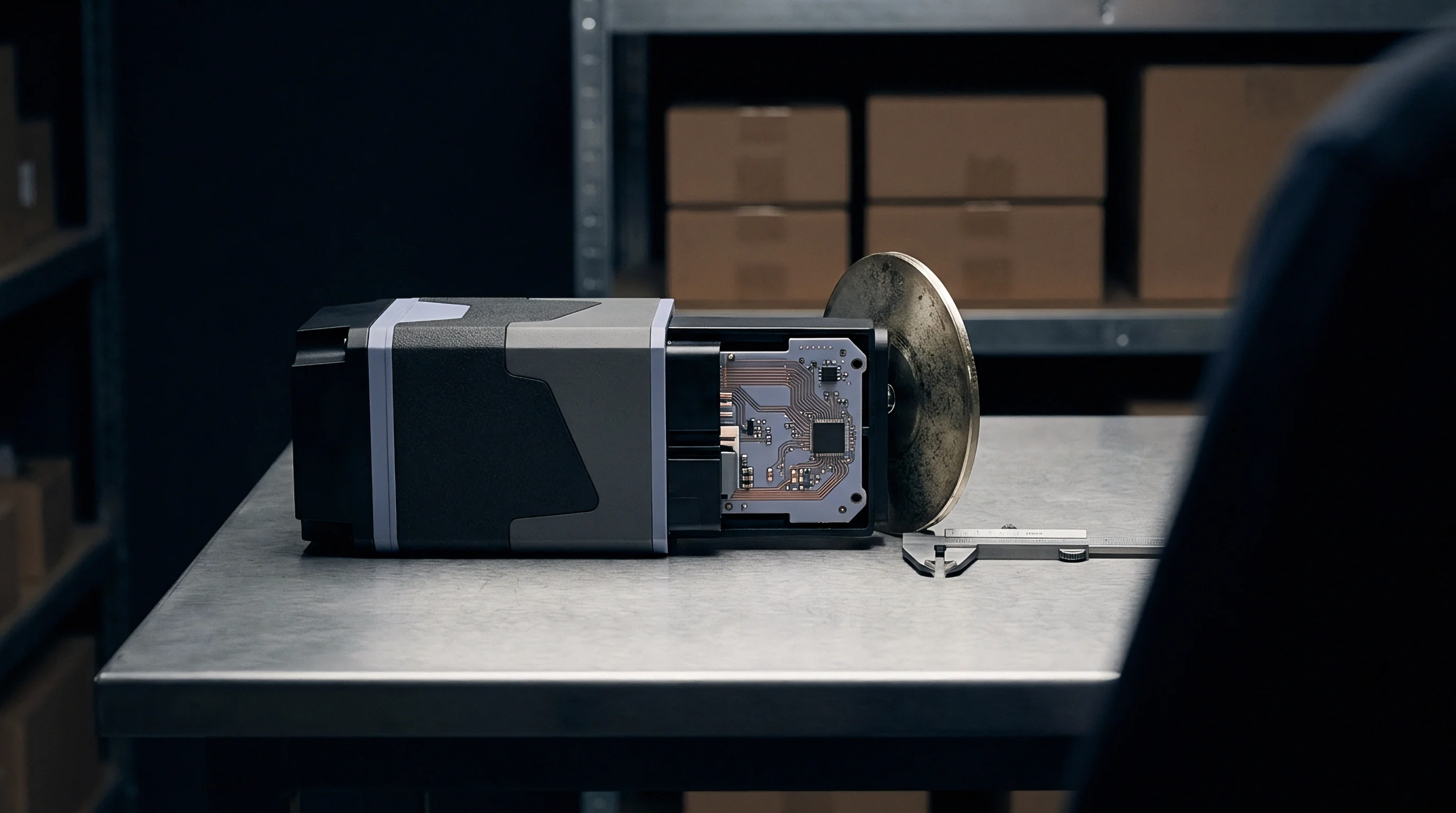
Physical shielding provides the final line of defense against radiated noise coupling into cellular antennas. Metal shield cans placed on the board enclose noisy subcircuits, attenuating electric and magnetic fields through absorption and reflection. Thin, stamped boxes made of tin-plated steel, nickel-silver, or copper alloys cover power stages, microcontrollers, and memory chips.
Shield effectiveness depends on material conductivity, magnetic permeability, thickness, and the size of any openings.

Shield Can Openings and Thermal Apertures
Perforations added to shield cans for solder outgassing or thermal cooling degrade isolation if the holes are too large. Small circular apertures act as waveguides below cutoff. Cutoff frequency for a circular aperture in thin metal follows the formula:
f_cutoff = 175 / d
Where f_cutoff is in gigahertz and d is aperture diameter in millimeters. A three-millimeter ventilation hole exhibits a cutoff frequency of 58.3 gigahertz. Well below cutoff, attenuation through an aperture of diameter d in a shield of wall thickness t calculates through established wave decay equations:
A = 32 (t / d) + 20 log10( (1 / (2 pi f mu_0 d)) )
At 2.5 gigahertz, one-twentieth of a wavelength is six millimeters; once aperture dimensions approach or exceed this size, magnetic shielding drops off rapidly. Arrays of closely spaced one-millimeter holes provide thermal convection without compromising shielding effectiveness. Multi-compartment frame-and-lid shields can isolate noisy buck regulators from sensitive RF matching networks within a single footprint.
Conductive elastomers and beryllium-copper finger gaskets maintain continuous electrical contact along seams where ground lands meet cast metal enclosures. Gasket compression should stay between twenty and thirty-five percent around the full perimeter; under-compression allows localized seam gaps, forming slot radiators that leak switching harmonics into external antennas. Uniform clamping keeps these radiating paths sealed off from digital noise.