Managing Micro-Asperity Constriction Losses in Millimeter-Wave Test Socket Pins
Mitigating micro-asperity constriction in mmWave sockets requires gold-cobalt plating, 15 um wipe distance, and 25 cN force to hold insertion loss under 0.3 dB.
Constriction
Millimeter-wave signals traveling through automated test socket pins lose measurable power when microscopic surface peaks restrict true metal-to-metal contact. Above 24 GHz, electromagnetic energy travels within skin depths only hundreds of nanometers thick. When a socket probe tip mates with a solder ball or land pad on a device under test, the surfaces touch only at discrete micro-asperities, leaving the actual conductive cross-section as a tiny fraction of the apparent footprint.
Forcing high-frequency current through these constriction channels introduces localized resistance spikes, phase instability, and fluctuating RF insertion loss that degrade automated test accuracy.
Skin Depth and Real Contact Geometry
Between 24 GHz and 77 GHz, signal currents run through a surface layer less than 500 nanometers deep. Beryllium copper alloy contacts plated with hard gold, for instance, have a skin depth of approximately 0.32 micrometers at 60 GHz. Because surface roughness prevents uniform mating when two metals are forced together, conduction is restricted to high points across the interface.
Under standard handler actuation force, the sum of these microscopic asperities ~ the real contact area ~ accounts for just 0.01 percent to 1.5 percent of the nominal contact area.
As operating frequency climbs and skin depth shrinks, the real contact area remains minuscule, constricting signal currents and driving up localized resistance.
Unable to penetrate into the bulk substrate, RF energy has to crowd through the narrow neck of each contact bridge. This bottleneck reshapes local electric and magnetic fields, adding localized inductive reactance to the increase in ohmic resistance. At higher frequencies, the complex impedance of the micro-asperity interface comes to dominate overall pin attenuation, far outweighing the bulk DC resistance of the spring pin container.
| Frequency (GHz) | Skin Depth (nm) | Real Contact Ratio (%) | Constriction Resistance (mΩ) | Insertion Loss Delta (dB) |
|---|---|---|---|---|
| 28.0 | 460 | 0.85 | 42 | 0.12 |
| 39.0 | 390 | 0.62 | 68 | 0.24 |
| 60.0 | 320 | 0.31 | 115 | 0.48 |
| 77.0 | 280 | 0.18 | 185 | 0.82 |

RF Insertion Loss Mechanics at Sixty Gigahertz
Electromagnetic field simulations show that local current bottlenecks produce both thermal dissipation and impedance mismatches. When constriction resistance at the pin tip interrupts a 50-ohm transmission path across a pogo socket, the discontinuity drives reflection losses. At 60 GHz, a constriction resistance of 115 milliohms shifts characteristic impedance enough to degrade S11 return loss beyond negative 15 dB, undermining measurement repeatability from one automated test cycle to the next.
RF energy lost across the contact dissipates as heat, while phase distortion develops alongside the drop in signal amplitude.
At 60 GHz, a reduction in real contact area from 1.0 percent to 0.31 percent increases insertion loss by 0.48 dB across a standard 50-ohm socket interface.
Thermal dissipation at micro-asperity bridges compounds signal degradation during high-power RF burn-in or functional testing. Forcing high RF current densities through micro-scale contact paths generates localized Joule heating. As the plating material within the constriction zone heats up, its resistivity rises ~ creating a positive feedback loop that accelerates signal attenuation and causes phase measurements to drift over production runs.
Overlooking micro-asperity constriction leads directly to uncalibrated yield fallout, as socket-induced signal attenuation flags compliant semiconductor packages with false failures.
Topography
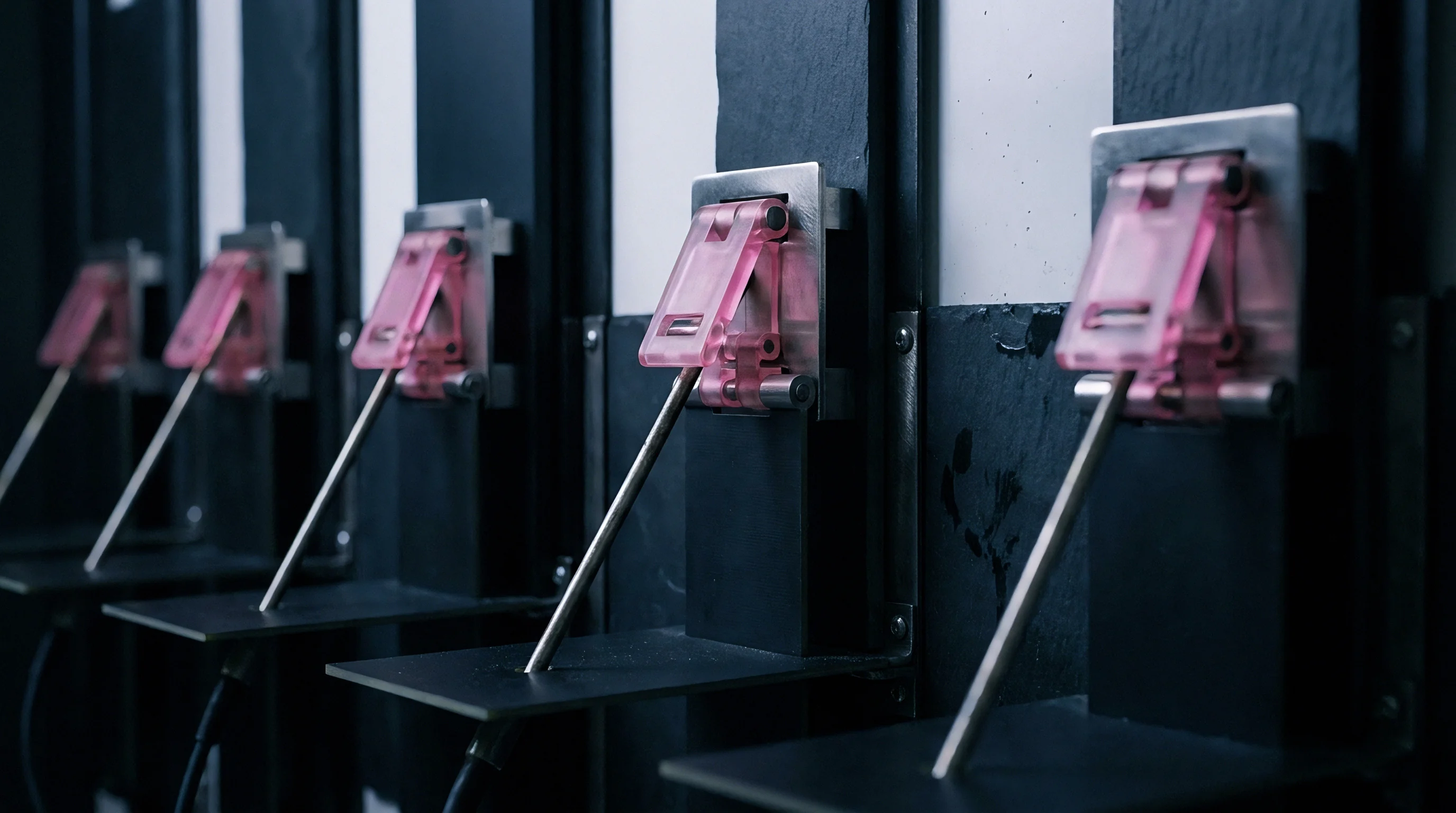
Surface profiles taken across probe pin tips show peak-to-valley variations that dictate how mechanical loads concentrate across high points. The distribution of asperities reflects statistical height variations set by polishing methods, plating chemistry, and post-machining steps. In socket pin specifications, these micro-topography parameters determine how the outer plating layers deform the moment they touch component lands or solder balls.
Plating Morphology and Asperity Micro-Yielding
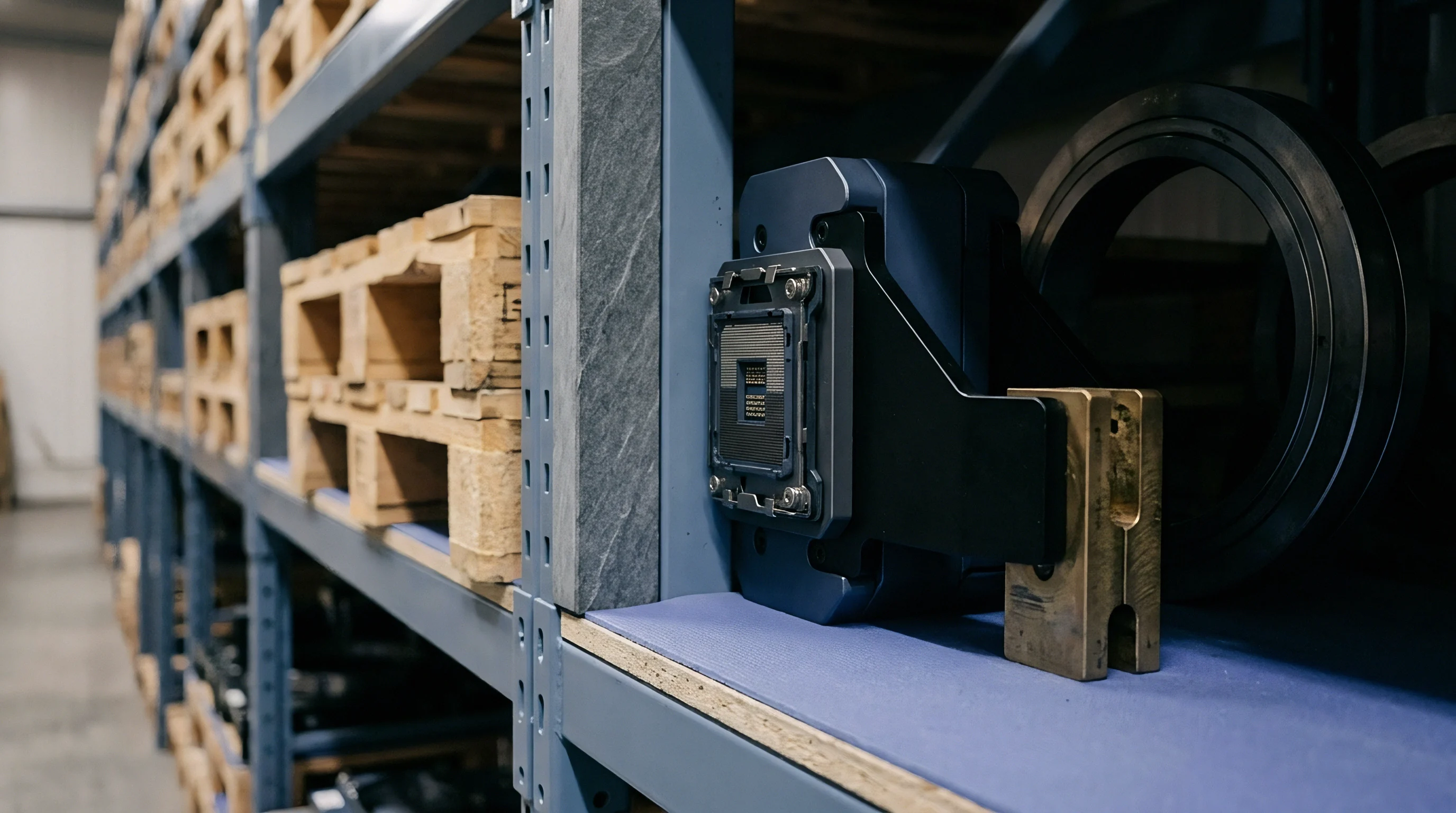
Hard gold plated over a nickel diffusion barrier forms a crystalline grain structure that yields under mechanical clamping. As contact force compresses asperities, localized stress quickly reaches the yield point of the softer metal, causing asperity tips to deform plastically and expanding the real contact area until the interface supports the load elastically ~ though hard gold plating significantly restricts this micro-yielding.
Electroplated gold-cobalt surfaces maintain hardness values between 140 and 200 HV. That hardness limits plastic flow, keeping individual asperity footprints small while preserving the finish over tens of thousands of insertions. By contrast, electroless nickel immersion gold deposits are noticeably softer; they yield quickly into larger initial contact areas, but wear down faster and succumb to oxidation under extended cycling.
| Plating Structure | Hardness (HV) | RMS Roughness (nm) | Skin Depth at 60 GHz (nm) | Initial Contact Resistance (mΩ) |
|---|---|---|---|---|
| Hard Gold (Au-Co) | 180 | 45 | 315 | 35 |
| Soft Gold (Pure Au) | 80 | 90 | 315 | 18 |
| Palladium Nickel (PdNi) | 350 | 30 | 440 | 85 |
| Rhodium (Rh) Over Ni | 600 | 25 | 290 | 110 |
Surface Roughness Metrics for High Frequency Pins
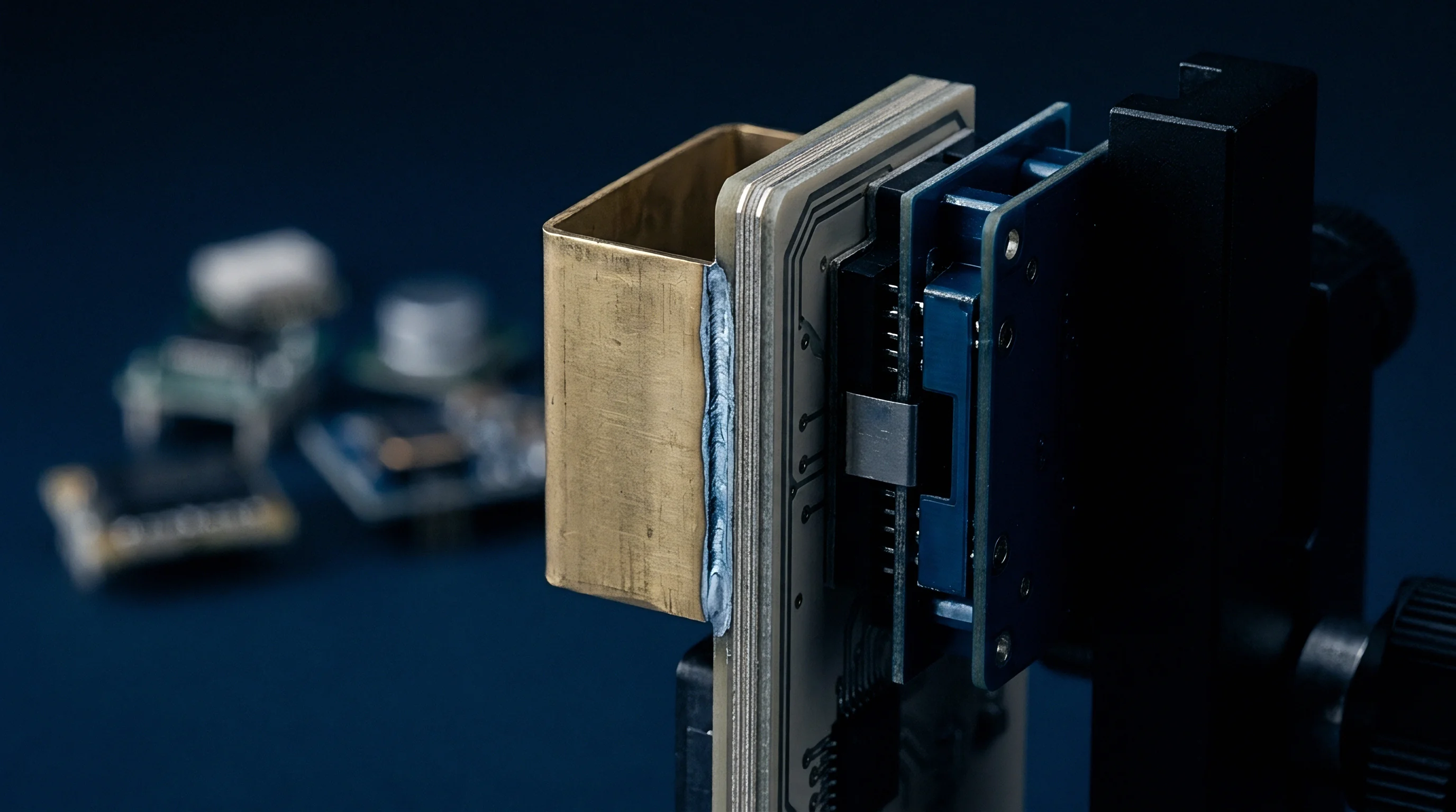
Arithmetic mean deviation figures give a misleading picture of actual conduction area because they ignore peak sharpness. Standard Ra roughness values average out surface profile swings without flagging the sharp micro-summits that drive constriction resistance. Specifying millimeter-wave socket pins therefore requires root-mean-square roughness and peak density metrics to gauge interface quality accurately.
Clamping force alone cannot overcome poor surface roughness, leaving cleanliness as the primary factor in maintaining stable impedance.
Increasing mechanical scrub distance removes surface oxide layers faster than increasing static contact force alone.
Combining high peak density with low root-mean-square roughness creates numerous micro-asperity contacts in parallel. Under basic network laws, splitting current across these parallel conduction paths lowers total constriction resistance. Establishing hundreds of tiny contact bridges curtails both ohmic loss and localized inductance across the pin tip interface.
- Asperity Crest Flattening permanently alters tip geometry, widening contact bridges and shifting RF reflection coefficients over time.
- Plating Flaking and Debris Accumulation traps non-conductive particles inside surface valleys, cutting off parallel conduction channels.
- Substrate Interdiffusion allows underlying copper or nickel to migrate through micro-cracks in thin gold layers, creating resistive oxide crusts.
- Fretting Wear Corrosion introduces microscopic slip cycles that grind surface oxides directly into the constriction path.
Relying on higher spring force to offset coarse surface finishes overlooks the resulting mechanical damage and accelerated gold transfer brought on by excessive tip pressure.

Load
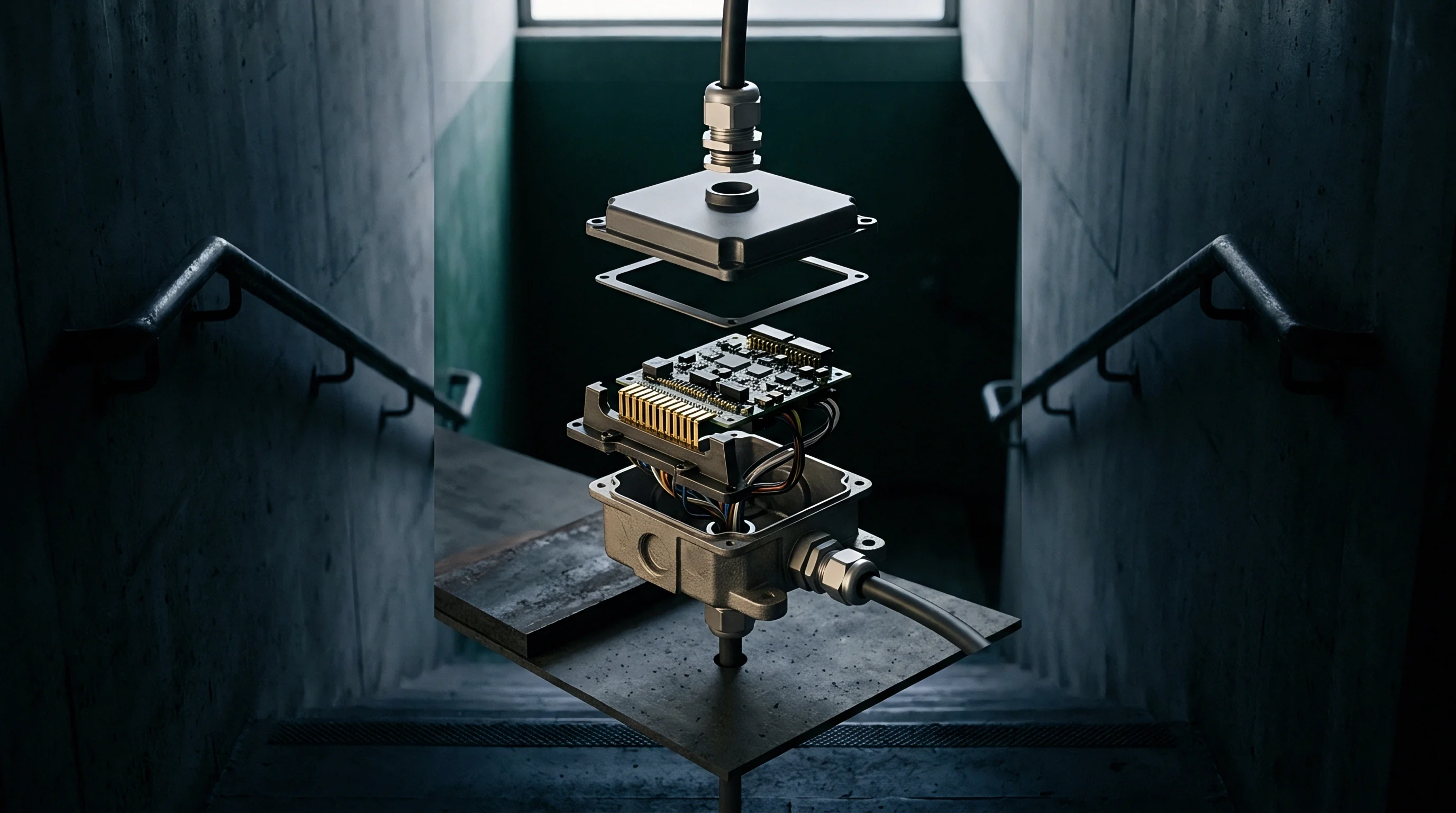
Actuation force from the test handler provides the mechanical pressure needed to flatten microscopic peaks at the interface. Finding the line between contact force and pin durability is central to high-frequency hardware design: excessive load crushes pin tips and damages device solder balls, while too little force leaves asperities barely touching, driving up constriction resistance and dropping signal levels.

Hertzian Stress Limits across Spring Elements
Cantilever and pogo springs deliver consistent force profiles across 100,000 cycles provided they stay within elastic limits. That deformation adheres to Hertzian contact stress mechanics: as a spherical pin tip meets a flat printed circuit board pad, the contact radius grows with the cube root of the applied force, and constriction resistance falls in inverse proportion to that radius.
Thermal expansion alters pin loading in production fixtures, compounding the mechanical wear that pogo pins experience over time.
- Align the handler plunger socket nest to within 3 micrometers of total indicator reading across the test socket mounting plate.
- Apply an initial preload stroke to verify uniform pin deflection across all high-frequency signal positions.
- Measure baseline contact resistance with a four-wire Kelvin sense setup before applying RF drive power.
- Advance the actuation carriage through the full wipe trajectory to shear ambient oxide films from mating surfaces.
- Record final insertion loss and return loss across the target millimeter-wave frequency band to verify interface stability.
Wipe Distance Control in Production Test Fixtures
Using lateral scrub to break through thin surface oxides demands mechanical alignment within 5 micrometers. As the pin compresses vertically, it slides horizontally across the device contact pad, shearing away non-conductive oxides and organic residues to expose fresh metal at individual asperity summits.
While wipe action shears away surface films, any exposed base nickel oxidizes rapidly once stripped.
| Force per Pin (cN) | Wipe Distance (µm) | Real Contact Ratio (%) | S21 Loss at Cycle 1 (dB) | S21 Loss at Cycle 50,000 (dB) |
|---|---|---|---|---|
| 15 | 5 | 0.22 | 0.55 | 1.25 |
| 25 | 15 | 0.45 | 0.32 | 0.48 |
| 35 | 25 | 0.68 | 0.25 | 0.72 |
| 45 | 35 | 0.82 | 0.21 | 1.45 |
Compliance with IEEE 287 precision connector interface standards mandates verification of contact force stability under thermal cycling conditions.
Wipe distance has to balance film clearing against plating life. At 25 centinewtons of spring force, a 15-micrometer wipe clears films and keeps initial insertion loss low without cutting through the gold layer. Pushing wipe beyond 35 micrometers rapidly strips that gold cap, exposing underlying nickel that oxidizes under continuous cycling.
Procurement specifications for high-frequency socket pins enforce strict limits on allowable contact force drift under EIA-364-70 standards, binding suppliers to verified mechanical endurance metrics.

Atmosphere
Ambient conditions around automated test handlers dictate how fast exposed base metals develop insulating films. Relative humidity, ambient temperature, and atmospheric pollutants react continuously with contact materials. Moisture condensation on pin tips accelerates electrochemical oxidation right in the micro-asperity valleys that carry high-frequency currents.
Oxidation Kinetics in High Duty Automated Sockets
Continuous device testing generates heat that speeds oxidation of exposed nickel underlayers. High local current density creates thermal hotspots at micro-asperities, where bridge temperatures can run more than 40 degrees Celsius above the bulk pin body. This localized heat accelerates film growth, building up resistive metal oxides within hours of continuous socket operation.
Thickening oxide layers drive up interface attenuation, turning socket degradation directly into false rejects that erode yield.
Oxidation narrows the conductive metallic diameter of each asperity bridge. Current previously carried by copper or gold is forced to tunnel through or rupture thin dielectric oxide films. This adds non-linear voltage-current characteristics to the interface, generating intermodulation distortion products that corrupt receiver sensitivity measurements during automated screening.

Can Ultrasonic Scrubbing Prevent Insertion Loss Drift?
Automated solvent baths strip away loose organic debris from probe tips, but they do nothing to reverse micro-structural deformation. Ultrasonic agitation washes out oil films and clears dust from the socket housing, yet solvents cannot restore depleted gold plating or strip hard intermetallic compounds formed at overheated asperity bridges.
Excessive spring force accelerates gold plating transfer and exposes base nickel underlayers to rapid ambient oxidation.
Offline cleaning routines need to pair chemical decontamination with optical checks of tip geometry. Solvents wash away loose contaminants, but once asperity deformation exceeds practical thresholds, only reconditioning or pin replacement stabilizes the interface. Without fresh pins, an otherwise clean socket will continue to show erratic RF insertion loss.
- Dry Nitrogen Purge Enclosures isolate the socket interface from room humidity, retarding oxide growth across micro-asperities during elevated-temperature test runs.
- Automated Tip Scrub Cycles run abrasive strokes across ceramic burnishing pads to abrade stubborn oxide crusts off probe tips.
- Gold-Cobalt Alloy Selection offers better oxidation resistance than pure gold or palladium-nickel coatings through extended high-temperature screening.
- Controlled Temperature Test Environments curb the thermal swings that drive base metal migration through thin protective plating layers.
Whether real-time nitrogen purging slows micro-asperity oxidation enough to justify the expense of handler-level gas delivery remains an open question across high-volume packaging facilities.
Budget
The true cost of high-frequency socket hardware includes both initial cartridge procurement and yield hits from false rejects. On millimeter-wave test floors, managers evaluate performance by total test cost per shipped unit. Pins whose asperities break down quickly drive expenses through handler downtime, repeated retests, and frequent cartridge swaps.
Landed Socket Cost per Ten Thousand Contacts
Replacement intervals dictate the ongoing cost of keeping RF measurements repeatable. Precision millimeter-wave probe pins run between 12 and 45 US dollars per contact depending on frequency rating, internal spring design, and plating quality. Outfitting a full socket for a 64-pin millimeter-wave device represents an upfront hardware investment exceeding 1,500 US dollars.
If inferior plating lets micro-asperities degrade after just 20,000 insertions, maintenance labor and handler idle time rapidly outstrip the socket’s purchase price. Specifying resilient plating and calibrated wipe motion can push pin life out to 80,000 cycles, cutting hardware consumption by more than 70 percent over a production campaign.

Yield Penalties from Uncalibrated Resistance Spikes
False failures caused by degraded micro-conduction end up scrapping good millimeter-wave silicon. In high-volume packaging lines, a 0.5 percent uptick in false rejects from socket insertion loss spikes wastes tens of thousands of dollars a day in retesting and discarded devices. Uncalibrated constriction resistance cuts straight into operational margins.
A socket pin plating specification prioritizing high micro-hardness and precise wipe geometry yields lower landed test costs than buying low-cost replacement cartridges.
Upgrading socket pin specifications with gold-cobalt alloy plating and controlled-force spring elements pays off by keeping RF insertion loss stable over extended runs. Verifying contact topography and constriction resistance creates predictable maintenance intervals, shielding production yield from measurement drift at the socket interface.