Quantifying Long Term Contact Resistance Instability in High Actuation Frequency RF Test Sockets
High actuation frequency RF test sockets experience contact resistance instability through micro-fretting and oxide growth, corrupting signal integrity and yield.


Drift
In high-volume RF semiconductor packaging plants, automated test equipment subjects socket pins to relentless compression cycles that gradually degrade the contact interface. A clean test pin usually exhibits direct-current contact resistance below twenty milliohms during initial calibration. By fifty thousand actuations, a combination of micro-fretting corrosion, material transfer from device pads, and spring relaxation raises that baseline.
The resulting shift alters signal path impedance, throwing off noise figure calculations, power amplifier efficiency readings, and vector error magnitude measurements.
The connection between a device lead and a high-frequency socket pin depends on microscopic asperities coming into physical contact. Current concentrates through these tiny points, creating localized constriction resistance. When pins actuate more than three times per second, flash temperatures at these micro-contacts can reach several hundred degrees Celsius.
This heat speeds up film growth, turning clean conductive metal into resistive oxides. Over time, gold plating wears through to the underlying nickel or copper, exposing base alloys to ambient oxygen and humidity on the floor.
Intermetallic diffusion causes similar trouble during continuous RF module testing. Soft tin, lead, or silver from land-grid array pads wipes onto socket contact tips during mechanical scrub. Across tens of thousands of cycles, this transferred metal oxidizes into a dull crust.
At low DC voltages, the oxide layer acts as an insulator; at high radio frequencies, its non-linear behavior creates intermodulation distortion that distorts receiver sensitivity tests on integrated Wi-Fi 7 and cellular IoT modems.
Continuous high-actuation testing produces wear patterns quite different from those seen in static interconnects. Cycles of compression, friction, and release break off sub-micron wear debris that settles inside pogo pin spring cavities or cantilever flexure channels. As dust and metal particles pack into these tight spaces, spring travel narrows and normal force drops below what is needed to pierce native oxides on incoming package pads.
Lower force drives up interface resistance and leaves signals prone to mechanical vibration during handler moves.
Signal attenuation through a degraded socket scales non-linearly with frequency. At sub-gigahertz bands like 868 MHz or 915 MHz used by industrial sensor modules, a small rise in DC resistance adds almost no insertion loss to a standard fifty-ohm path. At 5.8 GHz, 24 GHz, or 60 GHz millimeter-wave frequencies, that same rise destabilizes impedance matching.
Parasitic capacitance across the thin oxide layer couples with local pin inductance to form an unexpected high-pass or notch filter, distorting wideband signals and dropping good silicon.
A contact resistance rise from 15 mΩ to 180 mΩ shifts the insertion loss of a 5.8 GHz test socket by 0.65 dB when operating into a 50 Ω load.
Tri-temperature testing compounds electrical instability through thermal movement. Evaluating RF power amplifiers at junction temperatures of eighty-five degrees Celsius pushes expansion stress straight into socket assemblies. Differing expansion rates across the liquid crystal polymer body, beryllium-copper spring pins, and silicon substrates force microscopic shifts across the contact interface.
This thermal micro-fretting scrapes away outer gold coatings and exposes base metals to rapid oxidation.
Contact tip breakdown follows distinct mechanical and chemical stages during automated handler operation:
- Plating Abrasion removes soft outer gold flash, exposing hard nickel underplates that exhibit higher resistivity and susceptibility to surface passivation.
- Solder Transfer Accumulation deposits low-melting-point alloys onto socket pin tips, generating resistive intermetallic layers under high-current radio-frequency transmit bursts.
- Spring Relaxation reduces pin wiping pressure over high cycle counts, preventing the contact tip from clearing debris during initial mechanical engagement.
- Oxide Passivation forms thin insulating films across exposed base metals, converting linear ohmic contacts into non-linear diode-like electrical junctions.
- Cavity Contamination traps particulate matter inside spring probe channels, causing erratic contact resistance spikes and sudden signal path open circuits.
High-power RF testing, such as front-end module characterization at plus thirty decibels relative to one milliwatt, turns elevated contact resistance into localized Joule heating. Extreme current densities passing through tiny contact points heat pin tips rapidly. The excess temperature softens the alloy, distorting the tip profile and accelerating wear in a feedback loop that pushes contact resistance beyond allowable yield limits.
Undetected socket resistance shifts carry immediate financial costs. False yield drops force test cells to run rejected parts a second time, wasting machine capacity and lengthening cycle times per unit. Unrecognized resistance growth causes the opposite error, letting out-of-spec radio modules pass through to assemblers and shifting failure risks down the supply chain.
Tracking resistance trends across high cycle counts lets test teams schedule pin swaps before yields suffer.
Early contact resistance increases stem primarily from raw material interface limits, though atmospheric humidity variations and solder ball contamination can also contribute.
Scrub
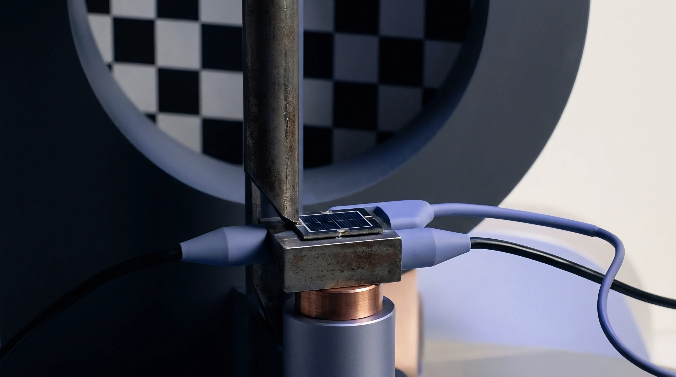
Mechanical wiping at the pin tip is the primary mechanism for breaking through surface oxides on package leads. As a device settles into the socket housing, the pin tip travels laterally across the contact pad over a calibrated distance. This scrub action cuts past organic residues and oxides to reach clean metal underneath.
Balancing this profile requires matching oxide penetration against pad wear and tip life over extended production runs.
Tip geometry controls how pressure concentrates during mechanical engagement. Crown tips, point tips, chisel edges, and spherical radii respond differently to package metallization. A sharp chisel edge generates high local pressure to cut through surface films under minimal normal force, but it digs deep into soft solder pads and creates debris that clogs the socket structure.
A spherical radius spreads force across a broader patch, protecting pad surfaces but demanding higher spring force to break through oxides.
Spring dynamics dictate resistance stability across multi-thousand cycle runs. Sockets are typically specified with initial spring forces between fifteen and thirty-five grams-force per pin based on device pitch and thermal constraints. Over two hundred thousand actuations, spring fatigue lowers normal force by ten to twenty-five percent.
Once spring force falls below critical limits, the tip can no longer clear surface films, causing DC contact resistance to bounce erratically between device insertions.
Finer pin pitches complicate scrub mechanics. High-density radio-frequency system-on-chip packages now feature pad centers spaced at 0.35 millimeters or less. Shrinking pin geometries cuts the cross-sectional area of internal spring coils, capping maximum spring force.
Micro-cantilever and conductive elastomer designs often replace helical spring pogo pins at fine pitches, but these alternative structures yield shorter scrub strokes, leaving them vulnerable to contamination buildup.
Alignment variations across automated test handlers directly affect scrub length. Thermal expansion in handler plunge heads, alignment pins, and load board circuit boards shifts device seating by tens of microns. Uneven mechanical plunging drives asymmetrical pin compression, producing inconsistent scrub across the array.
Pins with short scrub paths retain high interface resistance, while those pushed too far risk physical displacement from their guide channels.
Evaluating socket scrub requires analyzing both mechanical force and electrical metrics. The table below outlines key performance figures across common pin tip profiles used in high-frequency RF test sockets:
| Tip Geometry | Scrub Length (µm) | Normal Force (cN) | Debris Rate | Initial Rc (mΩ) | 100k Cycle Rc (mΩ) |
|---|---|---|---|---|---|
| Four-Point Crown | 35 to 50 | 220 to 280 | Moderate | 12 to 18 | 45 to 85 |
| Single Chisel Edge | 50 to 75 | 180 to 220 | High | 10 to 15 | 35 to 65 |
| Hemispherical Radius | 15 to 30 | 300 to 380 | Low | 18 to 25 | 110 to 240 |
| Micro-Cantilever Blade | 20 to 40 | 120 to 160 | Very Low | 25 to 35 | 140 to 310 |
Automated test routines must account for mechanical settle times after device insertion. Scrub movement generates dynamic resistance transients that take several milliseconds to clear once the plunge finishes. Fast handlers that start RF power sweeps before the mechanical interface settles capture noisy data, recording artificial gain variations and phase errors.
Adding precise dwell delays to the test sequence removes this settling artifact.
Contact surface roughness changes both friction behavior and wear rates over millions of actuations. Smooth, polished tips move with lower initial sliding friction, reducing mechanical stress on internal springs. However, highly polished contacts present larger true contact areas, making them susceptible to cold-welding when testing high-purity gold pads.
Controlled micro-texturing offers a middle ground, balancing sliding friction against metal transfer during long production runs.
Guide plate wear gradually shifts pin plunge trajectories over extended service cycles. Socket guide plates molded from liquid crystal polymers suffer abrasive wear from sliding pin shanks. As guide holes widen, pins tilt during compression, throwing off alignment and shortening effective scrub vectors.
This mechanical drift introduces channel-to-channel resistance skew across multi-port RF transceiver sockets, complicating parallel device testing.
Qualifying socket hardware for fine-pitch high-frequency packages demands clear mechanical checks. Key selection criteria include:
- Scrub Vector Verification confirms lateral tip displacement exceeds twenty-five microns under minimum specified plunging force to ensure surface oxide penetration.
- Plating Hardness Matching selects tip metallurgical coatings exceeding 200 Knoop hardness to prevent rapid tip flattening against hard device package contacts.
- Debris Clearance Channels verifies internal socket guide plates feature open clearance slots to prevent wear particle entrapment around moving spring shanks.
- Thermal Expansion Compensation checks socket material coefficients of thermal expansion match load board substrates to maintain alignment across extreme test temperatures.
Maintaining clean environmental conditions inside automated test cells limits debris problems. Air knife purge systems mounted to plunge heads blow dry nitrogen across socket arrays between insertions. Clearing loose metal flakes and dust before the next plunge prevents particles from packing into pin tracks, extending maintenance intervals.
Excessive scrub length cuts through pad plating to base copper, causing pin tips to scoop soft metal back into spring guide channels.

Physics
Signal propagation through an RF test socket follows high-frequency transmission line theory rather than standard low-frequency circuit rules. As frequencies move into the gigahertz range, current inside socket contacts compresses into a thin surface layer defined by skin depth. At 2.4 GHz, gold has a skin depth of roughly 1.55 microns, shrinking to 0.98 microns at 5.8 GHz and 0.48 microns at 24 GHz.
When mechanical wear strips outer gold plating, current shifts into higher-resistivity nickel or exposed copper alloys, pushing up surface resistance and insertion loss.
A socket interface can be modeled electrically as DC contact resistance in parallel with contact capacitance, tied in series with pin inductance. As surface oxides form, DC resistance grows while true physical contact area shrinks, altering interface capacitance. This complex impedance shift degrades return loss, altering S11 traces on vector network analyzers.
Transceivers with tight link budgets show apparent sensitivity loss when tested through sockets with degraded return loss profiles.
Local contact resistance growth creates impedance discontinuities along nominal fifty-ohm signal paths. Interface reflections generate standing waves along load board traces, corrupting EVM measurements on wideband Wi-Fi 6E signals using 160 MHz channels or Wi-Fi 7 channels using 320 MHz bandwidths. Reflected power travels back into the power amplifier output stage, altering load pull contours and causing good parts to fail production limits.
Phase noise testing on sensitive cellular IoT transceivers reacts strongly to minute resistance changes. Mechanical vibrations from automated handlers modulate contact resistance on worn pins, creating low-frequency resistance jitter. This fluctuation phase-modulates high-frequency RF signals passing through the pin, lifting the noise floor and causing high-tier GNSS or LTE-M modems to fail synthesizer specifications.
Evaluating how contact resistance changes affect RF performance requires measurements across defined frequency bands. The table below tracks insertion loss shifts, return loss degradation, and EVM noise additions against rising contact resistance levels:
| Frequency Band | Baseline Rc (15 mΩ) S21 (dB) | Degraded Rc (150 mΩ) S21 (dB) | Baseline S11 (dB) | Degraded S11 (dB) | EVM Floor Impact (% RMS) |
|---|---|---|---|---|---|
| 868 / 915 MHz (LoRaWAN) | -0.08 | -0.14 | -28.5 | -24.1 | +0.05 |
| 2.4 GHz (BLE / Wi-Fi) | -0.12 | -0.31 | -25.2 | -18.8 | +0.18 |
| 5.8 GHz (Wi-Fi 6E) | -0.22 | -0.78 | -21.0 | -13.4 | +0.62 |
| 24 GHz (5G FR2 mmWave) | -0.45 | -1.85 | -16.5 | -8.2 | +1.85 |
| 60 GHz (WiGig / Radar) | -0.85 | -3.40 | -12.1 | -5.1 | +3.50 |
Skin depth constraints concentrate power dissipation at contact boundaries during high-power transmit bursts. When a power amplifier outputs plus thirty-three decibels relative to one milliwatt into a fifty-ohm load through a degraded contact, current densities within the skin layer can exceed thousands of amperes per square millimeter. Joule heating in this thin zone rapidly heats the pin tip, driving thermal expansion pulses that induce further micro-fretting.
Ground return paths degrade rapidly when individual ground pins develop high contact resistance. High-speed RF ICs rely on parallel ground connections to keep ground loop inductance low. If specific ground pins form surface oxides, return current redistributes unevenly across remaining functional paths.
This asymmetric ground return increases inductive cross-coupling between adjacent signal pins, corrupting channel isolation on integrated transceivers.
Non-linear contact resistance creates severe measurement distortion during low-level RF testing. Thin native oxides act like metal-insulator-metal tunneling diodes, displaying non-linear voltage-current characteristics under small-signal conditions. When low-power signals, like sub-GHz receiver sensitivity test tones down at minus one hundred and ten decibels relative to one milliwatt, pass through these interfaces, non-linear distortion generates spurious signals within the receiver band and corrupts noise floor figures.
Contact resistance instability involves coupled thermal, mechanical, and electromagnetic effects. Vector network analyzer sweeps capture total S-parameter degradation, but separating surface resistivity changes from physical pin displacement requires targeted calibration. De-embedding algorithms lose accuracy when interface parameters drift mid-test.
Socket contact degradation manifests first as intermittent packet error rate spikes during high-power Wi-Fi transmit bursts before showing static direct-current resistance shifts.
Debris and organic residue changing dielectric properties around socket cavities further alter high-frequency wave propagation. As particles pack into pin cavities, the effective permittivity around the pin shifts, altering transmission line characteristic impedance. This variation adds phase delay and distorts group delay across wideband signals.
Modeling dielectric changes alongside resistance drift provides a complete view of socket degradation.
Accurate modeling requires connecting microscopic surface mechanics with macro-level RF behavior. Maxwell stress forces acting on surface asperities during high-power pulses create micro-displacements that alter real contact area in real time. Standard static lumped-resistor models miss these power-dependent impedance shifts seen during wideband power amplifier testing.
How can test engineers mathematically separate intrinsic semiconductor yield loss from dynamic impedance variations caused by microscopic surface degradation inside high-frequency test socket contacts?

Metrology
Tracking contact resistance drift in high-volume production environments calls for structured metrology. Standard two-wire DC measurements are unsuited for this work, as lead resistance, trace impedance, and meter contacts mask micro-ohm changes. Four-wire Kelvin sensing isolates interface resistance by keeping force and sense paths separate, allowing accurate readings below fifty micro-ohms.
Implementing Kelvin sensing in an RF test setup introduces layout challenges. Force and sense traces must meet as close to the pin tip as physically possible without altering transmission line impedance at multi-gigahertz frequencies. Parasitic capacitance from sense lines can detune fifty-ohm load board traces, requiring RF coaxial relays or bias tees to isolate DC measurement circuits during active testing.
Dry-circuit test standards enforce low voltage limits to prevent punching through delicate oxides. Under EIA-364-23C standards, open-circuit test voltages are clamped below twenty millivolts DC, with current limited to one hundred milliamperes. This ceiling prevents electrical breakdown of thin surface films, ensuring measurements reflect actual interface condition rather than artificial breakdown paths.
In-situ monitoring tracks resistance changes without pausing production. Injected test signals on unused ground or power supply pins measure contact resistance on every insertion. Algorithms process these time-series trends, predicting remaining socket life and triggering maintenance halts before yield drops occur.
Executing repeatable Kelvin measurements across production stations follows a structured calibration routine:
- Disconnect high-frequency instrumentation using RF coaxial relays to isolate load board traces from direct-current sensing paths.
- Insert a precision gold-plated shorting calibration standard device into the test socket using the automated handler plunge mechanism.
- Apply a clamped 10 mA direct-current force signal through the primary current injection path while monitoring open-circuit voltage rails.
- Measure voltage drop across the contact interface using high-impedance sense channels routed directly to the socket land pattern.
- Record four-wire resistance values across all pin channels, logging baseline values to automated statistical process control databases.
- Re-engage high-frequency instrumentation relays, execute vector network analyzer SOLT calibration sweeps, and resume production device testing.
Vector network analyzer calibrations must account for shifting socket impedance. Standard SOLT or TRL calibrations performed at shift start drift out of spec as pins wear across thousands of actuations. Adaptive de-embedding algorithms use live contact resistance values to update error matrices, adjusting S-parameter corrections across extended runs.
Statistical process control metrics track resistance trends to separate systematic socket wear from isolated device contamination. Standard rules trigger socket maintenance when mean resistance shifts three standard deviations above baseline, or when absolute resistance exceeds fifty milliohms on critical paths. Real-time tracking avoids premature rebuilds from temporary contamination while catching degraded sockets promptly.
Compliance with EIA-364-23C requires dry-circuit resistance measurements to clamp open-circuit test voltage below 20 mV to prevent breakdown of thin insulating surface films.
Infrared thermography offers a direct visual check for high-resistance pins during high-power testing. Thermal cameras mounted over open socket frames capture localized Joule heating at degraded contacts. Pin tip temperature rises exceeding fifteen degrees Celsius above ambient spot failing channels before return loss shifts show up on yield dashboards.
Sub-millimeter wave testing presents unique metrological hurdles due to physical size constraints. At 60 GHz, physical pin dimensions prevent routing traditional parallel Kelvin sense traces to pin tip contacts. Metrologists deploy high-frequency reflectometry techniques, monitoring phase shifts of high-frequency reflection coefficients to indirectly infer contact resistance changes based on calibrated physical-to-electrical interface degradation models.
During a high-density sub-GHz module test program, test operations absorbed a twelve-thousand-dollar load board destruction event when unrecognized contact resistance growth on a high-current supply pin caused localized thermal runaway, melting the liquid crystal polymer socket body and fusing test pins into inner PCB copper layers.
Mitigation
Extending socket life while keeping contact resistance stable relies on targeted metallurgy and durable plating selection. Standard soft gold over copper-beryllium offers low initial resistance but wears quickly under constant scrub. Modern contact designs use hard gold alloys modified with cobalt or nickel, reaching Knoop hardness values between 140 and 220 to slow mechanical abrasion during high-volume runs.
Alternative platings improve resistance to metal transfer and intermetallic growth. Palladium-nickel alloys topped with a thin gold flash create a tough, corrosion-resistant barrier that can outlast standard gold coatings threefold. For severe high-cycle applications above five hundred thousand actuations, rhodium and platinum-group coatings provide exceptional surface hardness and oxidation resistance, though their higher bulk resistivity requires optimized pin geometry to manage insertion loss.
Which Plating Metallurgy Resists Oxide Accumulation Longest?
Conductive diamond-like carbon and nanostructured coatings represent recent developments in contact protection. Applying thin conductive diamond-like carbon films onto beryllium-copper pin tips drops sliding friction below 0.1, curbing micro-fretting and preventing solder pick-up during high-temperature testing of lead-free packages. These coatings maintain stable contact resistance over millions of cycles in automated cells.
Comparing contact metallurgy parameters helps engineering teams match pin selection to operational requirements. The table below summarizes hardness, temperature limits, wear life, and cost factors across key contact platings:
| Plating Metallurgy | Hardness (Knoop) | Max Temp (°C) | Oxidation Resistance | Rated Actuations | Relative Cost Factor |
|---|---|---|---|---|---|
| Hard Gold (Au-Co/Ni) | 140 to 220 | 150 | High | 100,000 to 250,000 | 1.0x |
| Palladium-Nickel (PdNi+Au) | 350 to 450 | 200 | Very High | 300,000 to 600,000 | 1.35x |
| Rhodium (Rh) | 600 to 800 | 300 | Extreme | 750,000 to 1,500,000 | 2.10x |
| Conductive DLC Film | 1000 to 1500 | 250 | Immune | 2,000,000+ | 3.40x |
Automated cleaning cycles maintain socket health without removing load boards from the line. Every five hundred to two thousand actuations, handlers plunge test heads into micro-diamond abrasive pads or solvent-infused brushes. This step strips away solder debris, organic films, and loose particles, resetting the contact surface and controlling resistance drift.
Controlling environment inside automated handlers suppresses oxidation rates during continuous production. Purging sealed test enclosures with dry nitrogen keeps relative humidity below five percent and displaces oxygen. Running in an inert environment halts fretting corrosion on exposed base metals, allowing worn pins to stay within electrical specification longer.
Preventive maintenance relies on explicit qualification specs defining operational limits. Procurement documentation should require:
- Metallurgical Certification Reports document minimum plating thickness, underplate layer composition, and hardness testing results for incoming pin batches.
- Mechanical Force Curves chart normal contact force versus compression distance across initial, mid-life, and end-of-life actuation milestones.
- Cleaning Protocol Specifications define authorized solvent chemistries, abrasive pad grit sizes, dwell times, and maximum automated cleaning frequency parameters.
- Replacement Criteria Thresholds state absolute upper limits for direct-current contact resistance and maximum allowable return loss degradation before mandatory pin replacement.
Smart sockets incorporate micro-sensors to track mechanical health in real time. Strain gauges in socket housing walls monitor spring force degradation, while thermocouples monitor pin array heating during sustained power testing. Logged data routes directly to factory MES software, scheduling maintenance before contact wear leads to false rejections.
A standard procurement master service agreement clause stipulates that socket suppliers must guarantee contact resistance stability within plus or minus fifteen milliohms of baseline up to two hundred thousand actuations, or absorb full financial responsibility for all automated test handler re-test costs and replacement load board assemblies.

Economics
Managing contact resistance stability involves balancing socket hardware capital expenditure against operational yield metrics. High-performance RF sockets for multi-gigahertz ICs cost between three thousand and fifteen thousand dollars depending on pin count, operating frequency, and plating options. Cutting initial socket costs by opting for thin gold-flash designs often backfires, driving up operational expenses through frequent maintenance downtime and short pin lifespans.
False yield loss caused by worn socket contacts carries severe financial penalties in high-volume manufacturing. If an eighty-milliohm contact resistance adds half a decibel of false insertion loss to a Wi-Fi 7 power amplifier test path, good silicon drops below power output specs and gets rejected. In a line running one hundred thousand chips per week at four dollars per unit, a two percent false-reject rate burns eight thousand dollars weekly ~ far exceeding the cost of a premium hard-plated socket.
Re-testing rejected devices compounds operating expenses. Re-running parts through automated handlers consumes machine capacity, increases labor hours, and subjects delicate package leads to additional mechanical stress. Operating secondary test loops costs between twelve and thirty cents per unit, directly eroding gross margins and cutting throughput.
Evaluating total cost of ownership across socket options requires accounting for unit purchase price, cleaning consumables, maintenance labor, and yield protection. Upgrading to palladium-nickel or conductive DLC coatings increases initial purchase cost by thirty to two hundred percent, but extends operational life from one hundred thousand to over one million actuations. This extended lifecycle drops hardware cost per insertion to micro-cents while holding yield steady.
Scheduled pin replacements balance maintenance labor against the risk of catastrophic failure. Running sockets until pins fail completely risks thermal runaway that can destroy load boards, forcing days of downtime and costly board rebuilds. Scheduled pin swaps performed during planned maintenance avoid unscheduled outages and keep production moving.
Supply chain management for high-use test sockets relies on qualified second-sourcing and adequate safety stock. Pin dimensions and spring rates must match tight tolerances across vendors to guarantee drop-in electrical performance. Having a second qualified supplier prevents line halts during vendor delays or material shortages.
Yield tracking software tied to automated test cells gives line managers clear visibility into socket financial performance. Mapping resistance drift against device binning trends allows sourcing teams to hold socket vendors to contractual yield agreements, preserving profitability across high-volume RF packaging operations.
Establishing clear commercial alignment between test operations teams, socket vendors, and module buyers ensures capital commitments deliver optimal yield protection across global manufacturing locations.