
Trap Rich Layer Physics for RF Silicon Substrates
Trap-rich polysilicon layers beneath buried oxide pin interface carriers to eliminate parasitic conduction and lower sub-6 GHz harmonic generation.
Trap-rich polysilicon layers beneath buried oxide pin interface carriers to eliminate parasitic conduction and lower sub-6 GHz harmonic generation.
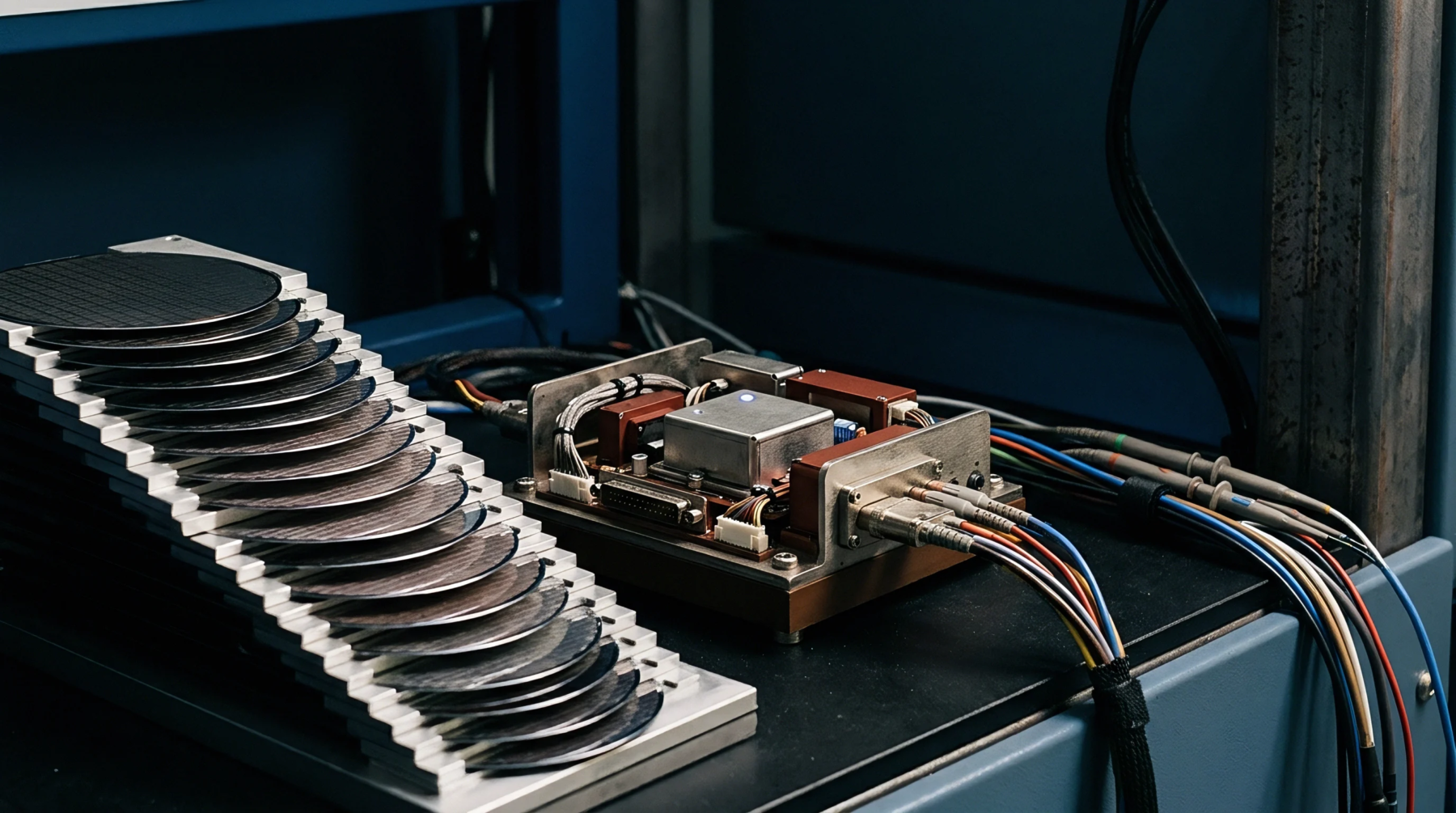
Dielectric breakdown modeling on trap rich silicon requires temperature adjusted voltage acceleration factors to prevent early RF switch gate oxide failure.

Trap rich polysilicon layers freeze interface charges to hold high resistivity and suppress switch harmonics below minus eighty dBc.
Expertise is a utility, not a secret. sentiention™ publishes its working knowledge as open reference: intelligence layer covering the materials it sources, the markets it enters, and the reference that serves both.