Chipset End of Life Notices and the Redesign Clock
A silicon end-of-life notice demands an immediate audit of last-time-buy volumes against redesign lead times to prevent production gaps during recertification.


Cadence
An End-of-Life notice on a primary wireless transceiver starts a financial countdown well before an engineer opens a schematic. Foundries schedule semiconductor process retirements around wafer volume dynamics, tooling depreciation, and fab conversions from legacy nodes like 90 nanometer planar CMOS to 22 nanometer planar or FinFET processes. When a foundry terminates wafer runs for a legacy radio System-on-Chip, the module vendor issues a Product Discontinuation Notice to device builders.
This notice fixes two non-negotiable milestones: the Last Time Buy deadline and the Last Time Ship deadline. While JESD48C defines a standard twelve-month window to the purchase order cutoff followed by six months to final physical delivery, commercial wireless suppliers regularly compress this to six months for order placement and three months for delivery when raw silicon allocations collapse abruptly.
An unannounced component retirement cascades through every tier of hardware manufacturing. For OEMs supporting field deployments with ten-year service lives, existing inventory can evaporate within three quarters. The redesign clock tracks the time required to update schematics, modify PCB stackups, port firmware, clear regulatory testing, and validate factory assembly tooling before parts run out.
A mismatch between redesign milestones and Last Time Buy quantities creates a production gap that stalls assembly lines, breaches distributor agreements, and leaves field installations without replacement stock. Engineering teams routinely underestimate certification lab lead times, resulting in product launch delays while stock levels drop to zero.
The window between a silicon product discontinuation notice and final wafer allocation closure leaves zero margin for engineering iteration cycles.
Assessing the real operational impact requires looking beneath the RF shielding can into the lower tiers of the component supply chain. Module integrators mount third-party radio ICs onto sub-boards alongside crystal oscillators, front-end modules, and discrete passives. If the silicon vendor ends production of the base transceiver die, the module vendor must declare the complete assembly obsolete.
Product teams using surface-mount modules often assume the shielding can isolates them from upstream foundry dynamics. That assumption collapses as soon as a replacement module forces changes to pad layouts, pinouts, command sets, or power architectures.
The transition from legacy Bluetooth Low Energy transceivers to modern multi-protocol SoCs illustrates the extent of these hardware shifts. Early 2.4 GHz transceivers required external power management circuitry, basic direct-conversion architectures, and microcontrollers with tight flash memory limits. Current replacements incorporate high-efficiency DC-DC buck converters, complex matching networks, internal hardware for secure boot, and expanded memory layouts that fundamentally change physical layer driver control.
Moving to a modern radio chip alters antenna matching impedance, sleep current profiles, pin assignments, and driver API parameters, turning what seemed like a routine bill-of-materials update into a system architecture review.

Silicon Discontinuation Timeline Drivers
Foundry economics dictate component lifecycles long before radio module manufacturers notify their customers. Pure-play foundries continuously evaluate revenue yield per wafer square inch across fabrication lines. As automotive, consumer, and computing demands shift toward tighter process geometries, foundries convert 200 mm wafer lines running legacy lithography over to higher-margin power semiconductors or analog ICs.
Producing radio ICs on older 0.18 micron or 90 nanometer CMOS nodes becomes unprofitable at lower manufacturing runs. When wafer yields slip or substrate costs rise, silicon suppliers consolidate their product catalogs by sunsetting low-margin wireless transceivers.
Cellular connectivity components see even faster obsolescence cycles due to baseband modem integration and cellular network standard revisions. Cellular module manufacturers phase out legacy LTE Category 1, Category 4, and early narrowband LTE-M or NB-IoT hardware as 3GPP standards advance from Release 13 through Release 17 and onward. Modem manufacturers discontinue earlier silicon to free up engineering capacity for multi-mode 5G RedCap and satellite-capable designs.
This leaves infrastructure equipment operators facing mandatory redesign cycles every four to six years, meaning industrial hardware often outlives two or three generations of its underlying cellular transceivers.
Unplanned obsolescence also stems from supply failures at the sub-component level inside the module package. Discrete passives, temperature-compensated crystal oscillators, low-noise amplifiers, and RF switches inside a module can be discontinued independently of the main baseband processor. If an oscillator supplier drops a miniature package size used in a module layout, the module manufacturer may retire the entire SKU rather than redesign the internal substrate routing.
Hardware procurement teams must therefore track end-of-life notices across the discrete components on detailed module bills of materials.
Longevity commitments differ sharply between commercial and industrial-grade silicon vendors. Standard consumer-grade wireless suppliers provide no formal commitment to maintain production beyond immediate market demand. Conversely, industrial-focused vendors maintain longevity programs guaranteeing device availability for ten, fifteen, or twenty years.
These programs carry higher unit prices but protect medical, utility, and aerospace products from forced redesign cycles. Deploying low-cost consumer transceivers into industrial products leaves the hardware exposed to unannounced component discontinuations that derail production plans.

Quantifying Redesign Lead Times across Systems
Tracking the engineering schedule during a transceiver retirement requires an accurate breakdown of sequential redesign phases. Converting schematics from a legacy wireless transceiver to an alternate IC takes four to eight weeks of hardware engineering. Laying out the multi-layer printed circuit board, conducting internal peer reviews, routing RF transmission lines, and refining ground planes adds another six to ten weeks.
Board fabrication, parts procurement, surface-mount assembly, and prototype delivery introduce an additional four to eight weeks. This initial hardware phase alone consumes nearly half of a standard six-month Last Time Buy window.
Firmware migration and stack integration occur alongside prototype assembly but present considerable schedule risks. Updating low-level hardware abstraction layers, driver calls, register definitions, and power state routines requires focused software work. When the replacement radio uses a different core architecture or command interface, application code must be re-architected to support the new SDK.
Protocol qualification for Wi-Fi 6, Bluetooth 5.4, or sub-GHz proprietary meshes demands weeks of lab verification covering packet error rates, link stability, duty cycles, and frequency hopping behavior. Firmware bugs identified during bench qualification can stall board sign-off for months.
| Protocol Category | Silicon Process Node | Typical EOL Notice Window | Redesign Sprint Duration | Recertification Lag | Supply Risk Level |
|---|---|---|---|---|---|
| Sub-GHz LoRa / Proprietary | 180nm to 90nm CMOS | 12 Months | 18 Weeks | 12 Weeks | Moderate |
| Bluetooth Low Energy / 802.15.4 | 55nm to 22nm ULP | 6 to 12 Months | 14 Weeks | 8 Weeks | Low to Moderate |
| Wi-Fi 5 / Wi-Fi 6 Dual-Band | 40nm to 16nm FinFET | 6 Months | 22 Weeks | 16 Weeks | High |
| Cellular LTE-M / NB-IoT | 28nm to 22nm FD-SOI | 3 to 6 Months | 26 Weeks | 20 Weeks | Critical |
Compliance testing and regulatory approvals represent the final bottleneck in the redesign schedule. Booking test time at accredited compliance facilities regularly requires six to eight weeks of advance notice. Radiated emissions testing, harmonic measurements, immunity testing, and radio standard verification require three to five weeks of chamber time.
If an RF layout issue produces an out-of-band emission spike, the team must spin the board, assemble new prototypes, and book a re-test. This testing delay frequently pushes total project delivery past the Last Time Ship deadline, causing production stockouts.
Vendors may market pin-compatible silicon to ease the transition away from a discontinued IC. While these chips match the existing PCB land pattern, they are rarely direct electrical drop-ins. Revised internal die layouts alter input impedance, register behavior, output stage performance, and firmware register maps.
Relying on pin compatibility without running a full RF parametric evaluation and a comprehensive firmware test suite routinely leads to degraded link budgets and field failures.
A full radio redesign cycle requires between eight and fourteen months under standard conditions. If component lead times for alternative silicon or specialized passives extend past twenty weeks, the schedule slips further. Engineering teams must compare project velocity against remaining Last Time Buy inventory buffers.
If the engineering timeline outlasts the silicon delivery window, procurement must secure additional inventory to prevent factory shutdowns.
How far can an engineering team compress regulatory testing lead times when silicon allocations drop unexpectedly without adequate last-time-buy inventory?


Silicon
Replacing an obsolete wireless transceiver IC with a newer die architecture introduces radio frequency variations that pass basic continuity testing unnoticed. Direct conversion homodyne architectures process signals differently than low-intermediate-frequency designs, altering how front-end amplifiers handle adjacent blockers and out-of-band interference. Local oscillator phase noise profiles vary between silicon generations, directly shifting receiver adjacent channel selectivity.
Swapping an older transceiver with integrated analog filtering for a modern digital-intensive architecture also shifts harmonic distortion profiles across temperature extremes, requiring RF engineers to verify that the replacement holds critical link margins.
Transmitter linearity and error vector magnitude change when baseband blocks migrate to smaller process nodes. Modern low-voltage processes run on core rails down to 1.1 volts, requiring integrated power amplifiers to rely on internal charge pumps or switching regulators. These switching stages inject narrow-band spurs into the RF path unless isolated by external decoupling networks.
A replacement IC might match the original +20 dBm peak output power on a summary datasheet, yet produce spectral regrowth and degraded EVM under complex modulation schemes like 1024-QAM Wi-Fi or 64-QAM cellular traffic.
Receiver noise figures govern overall system sensitivity limits in weak-signal environments. A 1.5 dB increase in noise figure measurably reduces cell coverage, generating dead spots in deployed networks. Silicon matching structures also differ between generations; an older part might use a differential 100-ohm balanced RF port, while its modern replacement provides a single-ended 50-ohm port with an on-die BALUN.
This physical change alters parasitic coupling to adjacent traces and ground planes, shifting receiver sensitivity and noise immunity.
On-die power management units introduce sharp current transients during operational state changes. Switching transceiver chips changes peak current demand during transitions from sleep to active transmission, affecting decoupling capacitors and supply rail stability. Modern transceivers use fast-locking phase-locked loops to shorten wake cycles, jumping from microamp sleep currents to hundreds of milliamperes during transmission bursts.
If the board power distribution network cannot supply these transients, voltage drop triggers brownout resets or corrupts baseband frame processing.

Radio Transceiver Architectural Variances
Evaluating receiver front-end performance requires checking how low-noise amplifier architectures have evolved between chip generations. Earlier transceivers relied on external discrete inductors and high-Q capacitors for off-chip filtering ahead of the first amplifier stage. Current wireless SoCs integrate matching networks on the die using compact spiral inductors with lower Q factors.
While this cuts external component counts, it degrades front-end selectivity, leaving the low-noise amplifier vulnerable to cross-modulation from strong out-of-band cellular or industrial signals.
Local oscillator architecture changes also shift wireless link performance over temperature. Fractional-N synthesizers in newer ICs offer fine channel resolution and fast settling times, but fractional spur generation can align with adjacent channel boundaries under certain temperature-dependent divide ratios. If these discrete spurs land on active channels, the design breaches out-of-band emission limits at high temperatures even if room-temperature bench sweeps look clean.
Replacing a legacy transceiver with a newer low-power radio IC can produce an 8 dB surge in second-harmonic emissions at 85 degrees Celsius, mandating an external low-pass filter revision.
Dynamic range limits in integrated analog-to-digital converters dictate how well a receiver tolerates in-band interference. Older radios relied on high-bit-depth sigma-delta ADCs with high oversampling ratios to maintain wide dynamic range in congested RF bands. Denser silicon designs frequently adopt lower-power successive-approximation-register (SAR) ADCs running at lower oversampling rates to reduce power consumption.
This trade-off cuts operational current but limits interference rejection, increasing packet error rates near co-located transmitters or industrial machinery.
| Parametric Metric | Generation 1 Legacy IC | Generation 2 Drop-in IC | Generation 3 Modern SoC | Test Condition / Parameter |
|---|---|---|---|---|
| Rx Sensitivity (1 Mbps GFSK) | -93.5 dBm | -96.0 dBm | -98.5 dBm | BER 0.1%, 2.402 GHz, 25°C |
| Max Transmit Power | +4.0 dBm | +5.0 dBm | +8.0 dBm | Conducted, 50-ohm load |
| Tx 2nd Harmonic Emission | -48.0 dBm/MHz | -41.5 dBm/MHz | -36.2 dBm/MHz | Pout Max, 4.804 GHz sweep |
| Deep Sleep Current Draw | 1.20 µA | 0.85 µA | 0.35 µA | RAM retention, RTC active |
| Rx Sleep-to-Active Time | 350 µs | 180 µs | 85 µs | 32 MHz XTAL start to Rx lock |
| Adjacent Channel Rejection | 38 dB | 32 dB | 29 dB | +1 MHz offset, desired at -67 dBm |
Digital baseband modem filtering shifts between chip versions also alter signal recovery in fading channels. Earlier radios used dedicated hardware state machines with fixed finite impulse response filters tuned for specific symbol rates. Modern software-defined basebands on internal DSPs allow variable filter bandwidths across multiple modulation types.
However, misconfigured digital filter taps in ported drivers can widen the channel passband, allowing out-of-band noise to degrade sensitivity.

Transceiver Substitution Failure Modes
Unintended hardware interactions appear quickly when mounting alternative silicon onto existing circuit board layouts. Baseband lines, decoupling paths, and RF traces interact directly with modified package footprints. Minor pinout changes alter return paths, generating parasitic resonances that degrade transceiver metrics.
- Unmatched Input Impedance causes excessive RF power reflection at the chip interface, degrading total radiated power and receiver sensitivity figures.
- Power Supply Cross-Talk occurs when internal switching regulator harmonics leak into analog phase-locked loop circuits, raising phase noise levels.
- Thermal Drift Shift causes local oscillator frequency offset to drift outside receiver capture bandwidths under high operating temperatures.
- Drive Strength Mismatch on digital SPI or UART bus lines creates ringing and excessive electromagnetic interference on adjacent analog RF traces.
- Firmware Command Latency expands execution time for radio state changes, corrupting timing-critical protocol handshake frames.
- Incompatible Sleep States prevent lower-power operating modes from engaging correctly, draining system battery reserves within months.
Firmware abstraction layers can conceal critical physical layer control differences between radio silicon families. Legacy drivers might set output power using direct register hex values written to an internal amplifier stage. Running that driver logic on a replacement IC with a different gain-step architecture can saturate the transmitter or drop output power entirely.
Firmware engineers must reconstruct low-level abstraction layers to map power settings, clear channel assessment thresholds, and low-noise amplifier gain steps directly to the new device register map.
A hardware drop-in chip substitution remains incomplete until firmware register maps match the physical amplifier gain steps of the replacement silicon die.
Clock source compatibility is another regular failure point during transceiver replacement. Older transceivers frequently integrated oscillator inverter circuits tuned for high equivalent series resistance 32 MHz or 26 MHz crystals in larger packages. Modern low-power SoCs use oscillator circuits built for low-drive miniature crystals.
Retaining the legacy crystal network on a new layout can cause startup failures, crystal overtone oscillation, or frequency drift at cold temperatures that breaks protocol timing.
Thermal dissipation behavior shifts when migrating from Quad Flat No-lead (QFN) packages to Wafer-Level Chip-Scale Packages (WLCSP). Smaller package footprints reduce the ground pad area available to conduct heat into the PCB planes. Under high duty cycles or continuous transmission, junction temperatures in compact silicon climb rapidly, triggering internal thermal throttling or degrading power amplifier linearity during active packet bursts.
Migrating to denser silicon architectures requires validating every physical layer parameter across full industrial temperature and voltage ranges rather than assuming register compatibility across chip generations.


Trace
Re-routing PCB traces for a replacement radio IC introduces parasitic inductance and capacitance changes that alter high-frequency link margins. Monopole, inverted-F, and patch antennas rely on specific ground plane dimensions and clearance zones to maintain their tuned center frequency and radiation pattern. Changing trace widths, dielectric spacing, or via placements to accommodate an alternative pinout shifts the characteristic impedance of coplanar waveguides and microstrips away from the 50-ohm target.
An RF trace clearance change of 0.1 millimeter can detune the antenna matching network, shifting peak resonance by hundreds of megahertz and attenuating radiated power.
Multi-layer board stackups affect signal integrity through substrate thickness tolerances and dielectric constant variations. Standard FR-4 materials show dielectric constant shifts between 4.2 and 4.7 across fabrication lots and operating frequencies. When redesigning a PCB for an alternate transceiver, altering layer stackups or dielectric thicknesses requires recalculating coplanar waveguide gap dimensions.
Failing to adjust layout geometry for substrate properties introduces transmission line impedance discontinuities, raising voltage standing wave ratios and radiating harmonic noise.
Via fences and ground return paths around RF traces require rebuilding during layout revisions. High-frequency return currents travel the path of lowest inductance directly below the signal trace on adjacent ground planes. Splitting ground reference planes with digital traces or signal vias forces return currents into wider loops that act as unintentional slot antennas.
Layout designers must place continuous via fences along microstrip boundaries at spacings tighter than one-tenth of the guided wavelength to contain RF fields and prevent coupling into power planes.
Adjusting component placement in the matching network shifts parasitic coupling and alters circuit Q factors. RF matching networks use small surface-mount inductors and capacitors arranged in pi or T configurations to transform complex die impedances to the 50-ohm antenna line. Moving a matching inductor 3 millimeters closer to a copper pour alters its effective inductance through eddy currents induced in the ground plane.
Re-routing an RF path during a redesign requires remeasuring component values with a vector network analyzer rather than carrying over schematic values from the previous revision.

PCB Stackup and Parasitic Management
Designing transmission lines on revised multi-layer boards requires tight control over trace geometries and plane separations. Single-ended microstrip traces on 1.6 millimeter four-layer FR-4 boards require widths near 0.5 millimeters over a solid layer-two ground plane with 0.2 millimeter dielectric spacing. Moving that design to a six-layer board with 0.1 millimeter outer dielectric layers narrows the required 50-ohm trace width down to roughly 0.18 millimeters.
Layout engineers must verify substrate dielectric thicknesses with the board fabricator before finalizing copper artwork.
Coplanar waveguides with ground (CPWG) offer stronger field confinement for high-density layouts undergoing transceiver replacement. CPWG structures flank the top-layer RF trace with ground copper separated by a defined gap, backed by a solid reference plane underneath. This profile limits coupling into nearby digital traces and shields against external interference.
The gap between the RF trace and ground pours must remain uniform along the route, avoiding narrow pinches near component solder pads.
Ground cutouts under RF matching components reduce parasitic capacitance to ground that degrades filter responses. High-value matching inductors and capacitors have self-resonant frequencies limited by their package size and pad capacitance to adjacent copper. Clearing layer-two ground copper directly below matching component pads lowers pad capacitance, shifting self-resonant points well above the operating frequency band.
Layout designers must balance these copper voids against the requirement for continuous return paths on surrounding routes.
Running digital lines such as SPI, I2C, or UART parallel to high-frequency RF traces introduces switching noise into the receiver front end. Fast clock edges on SPI buses generate harmonic energy reaching past 2.4 GHz, which couples into unshielded RF traces. Redesigned boards should place digital traces on internal layers between solid ground planes, crossing RF routes only at right angles when layer transitions are required.
Ground guard traces between parallel digital buses and sensitive analog RF lines provide additional isolation.
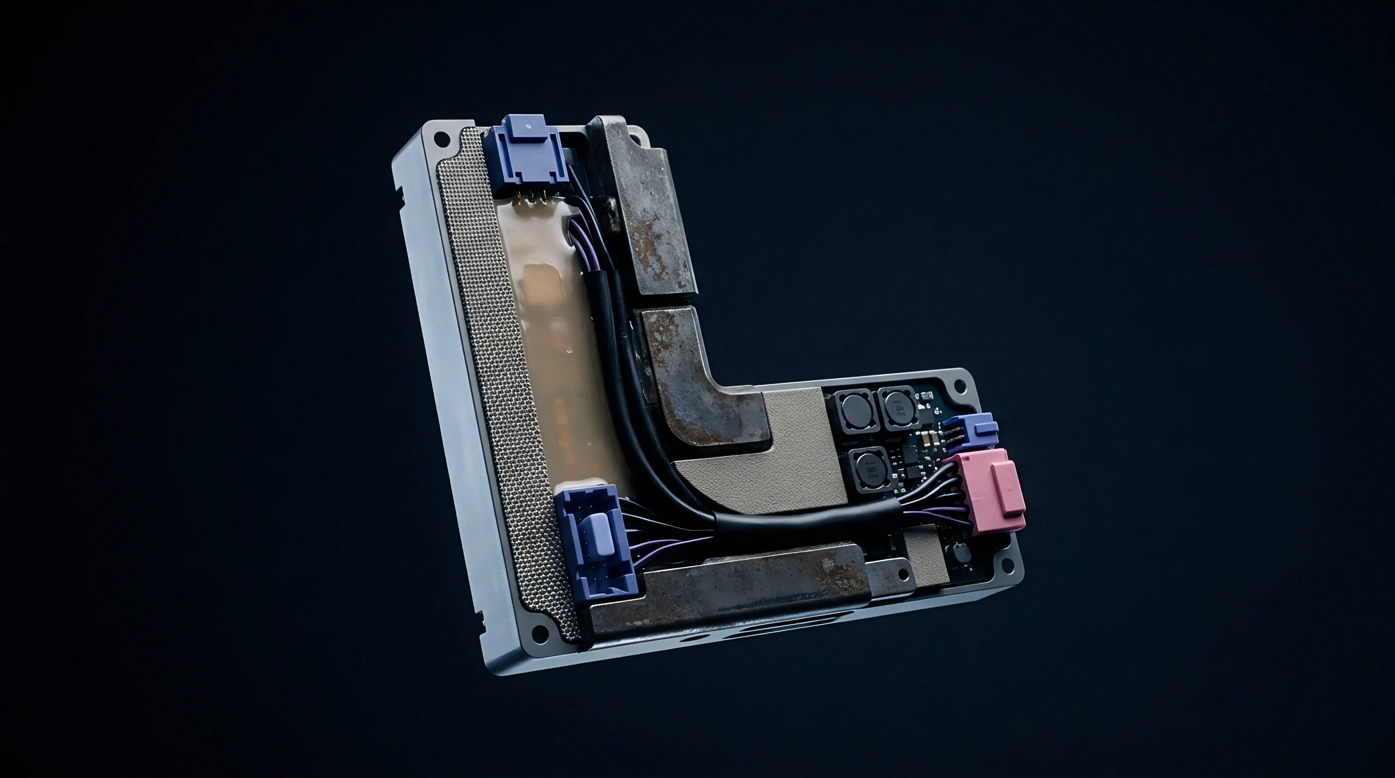
RF Network Matching Procedure
Re-matching an RF network following a transceiver footprint update requires a bench calibration process. Measurements must be taken systematically on unpopulated prototype boards using a calibrated vector network analyzer.
- De-embed Calibration Cables using a dedicated SMA test fixture to zero out cable phase shift and attenuation up to the board injection point.
- Isolate the Antenna Connection by removing downstream passives and soldering a coaxial pig-tail test connector directly onto the primary 50-ohm layout pad.
- Measure Uncompensated Chip Impedance across the operational frequency band while driving the transceiver output port in raw continuous-wave test mode.
- Synthesize the Pi-Network Values inside Smith chart simulation software to calculate exact series inductance and shunt capacitance values needed for 50-ohm match.
- Populate High-Q RF Passives on the matching pads, utilizing tight-tolerance 1% ceramic capacitors and wire-wound inductors with self-resonant frequencies well above operating bands.
- Verify Radiated Return Loss across the antenna terminal, confirming S11 return loss measures better than -15 dB across all active operating channels.
Antenna detuning caused by enclosure clearance shifts or relocated components is a frequent failure point in board revisions. Printed inverted-F antennas rely on ground plane dimensions to establish a resonant counterpoise. Altering primary PCB ground plane length by 5 millimeters during a footprint migration pulls antenna resonance away from the intended operating band.
Locating copper pours, battery terminals, or shielding walls near the antenna element loads the near field, absorbing energy and cutting radiated efficiency.
Shielding cans across revised layouts keep internal RF emissions away from baseband circuits and block ambient electromagnetic interference. Multi-cavity cans separate low-noise amplifier inputs from switching regulator inductors and digital processing buses. Solder pads along shield wall perimeters require continuous ground vias spaced no more than 2 millimeters apart.
Insufficient via stitching converts the shield frame into a re-radiating element that fails out-of-band emission tests.
An unverified PCB stackup change that detunes an internal loop antenna can drop link budget by 6 dB across industrial field sites, triggering a six-week project delay and forty-two thousand dollars in re-tooling costs.
Verifying trace revisions through conducted vector network analyzer measurements and full 3D chamber pattern sweeps catches link budget deficits before committing to volume tooling.


Approval
Changing silicon components or modifying PCB trace layouts in a certified radio assembly invalidates original regulatory approvals under spectrum compliance rules. Regulatory bodies like the Federal Communications Commission in the United States and notified bodies under the European Radio Equipment Directive apply strict frameworks to intentional radiators. When replacing an obsolete transceiver, manufacturers must establish whether changes qualify as a permissive change or demand a new equipment authorization.
Selling hardware under legacy certification numbers after making unapproved modifications breaches spectrum regulations, exposing the manufacturer to fines, customs holds, and product recalls.
United States regulations under FCC Part 15 specify conditions for Permissive Change submissions. A Class I Permissive Change covers minor alterations that do not increase radiated emissions or change fundamental RF parameters, requiring only internal records updates. Replacing a primary wireless transceiver IC rarely meets Class I requirements.
Most transceiver substitutions require a Class II Permissive Change, which requires formal laboratory data confirming that radiated spurious emissions and out-of-band mask compliance stay within certified limits. If the replacement IC increases conducted output power or alters modulation schemes, the FCC requires a full Equipment Authorization filing under a new FCC ID.
European compliance under the Radio Equipment Directive 2014/53/EU requires manufacturers to update the formal Declaration of Conformity dossier when internal radio components change. RED rules require technical documentation to include test reports verifying compliance with harmonized standards like EN 300 328 for 2.4 GHz systems or EN 300 220 for sub-GHz devices. While RED relies on self-declaration supported by a technical construction file, changes impacting spectrum efficiency, electromagnetic compatibility, or safety require re-testing at an accredited laboratory before applying the CE mark to updated assemblies.
Cellular hardware faces commercial certification requirements beyond government spectrum regulations. Mobile carriers require PTCRB or GCF network conformance certification for devices operating on commercial cellular networks. When an obsolete cellular module is replaced, the device manufacturer must complete PTCRB delta testing to verify antenna performance, spurious emissions, and SIM electrical stability.
Individual cellular carriers also mandate proprietary acceptance testing before permitting redesigned hardware to connect to their LTE-M or NB-IoT networks.

Regulatory Filing Categories and Rules
FCC Permissive Change filings require technical comparisons between original baseline measurements and redesigned prototype data. A Class II Permissive Change preserves the original FCC ID, avoiding label changes and enclosure tooling updates. To qualify, the replacement silicon must be pin-compatible or electrically equivalent, using identical modulation schemes, channel bandwidths, and peak power ratings.
Submissions must include radiated emissions scans through the tenth harmonic of the fundamental frequency.
Modular Approval rules simplify obsolescence management if the original design used a certified wireless module. Full modular approval allows swapping an obsolete module for a certified replacement without re-running system-level intentional radiator testing. However, modular approvals apply only if the host PCB antenna type, gain, and microstrip layout adhere to the module manufacturer’s original grant terms.
If the host design modifies the antenna trace or incorporates a higher-gain antenna, host-level permissive changes or full recertification are required.
| Regulatory Jurisdiction | Filing / Assessment Type | Required Test Scope | Average Lab Cost (USD) | Typical Lead Time |
|---|---|---|---|---|
| USA (FCC) | Class II Permissive Change | Radiated Spurious, Band Edge | $4,500 – $7,500 | 3 to 5 Weeks |
| USA (FCC) | New Equipment Authorization | Full Part 15 Radiated & Conducted | $12,000 – $18,000 | 6 to 8 Weeks |
| Europe (EU RED) | Updated Technical File / DoC | EN 300 328 / EN 301 489 Recertification | €5,000 – €9,000 | 4 to 6 Weeks |
| Global Cellular | PTCRB Delta Certification | 3GPP Conformance, Radiated Spurious | $15,000 – $35,000 | 6 to 10 Weeks |
| Japan (MIC / VCCI) | Category Modification Filing | Radio Law Article 2 Paragraph 1 | ¥600,000 – ¥900,000 | 4 to 7 Weeks |
Specific Absorption Rate (SAR) testing introduces additional requirements for wearable and handheld devices. If a component change alters power control logic, RF matching, or component proximity to the enclosure wall, SAR distribution shifts. Transmitters operating within 20 centimeters of the body must prove exposure compliance under current test protocols.
If localized SAR values exceed limits, transmit duty cycles must be limited in firmware, lowering effective throughput.
Standard revisions occurring during a redesign cycle can force legacy products to comply with newer, stricter requirements. Regulatory bodies establish transition deadlines after which older test standards expire. If a design requires a Class II filing after a standard transition date, the laboratory must evaluate the hardware against the new requirements.
These standard updates regularly tighten out-of-band emission limits or receiver blocking thresholds that older circuit topologies struggle to meet without broader board changes.

Documentation Dossier Requirements
Submitting an application to a Telecommunication Certification Body requires compiling hardware test data, schematic revisions, and operational descriptions into a structured package.
- Detailed Circuit Block Diagram detailing local oscillator frequencies, internal mixer stages, filter bandwidths, and power distribution paths.
- Updated Schematic and Bill of Materials highlighting exact component substitutions, package variations, and revised passives within RF paths.
- PCB Gerber Files and Stackup Specs confirming trace width adjustments, ground plane structures, and coplanar waveguide gap dimensions.
- Engineering Rationale Letter detailing the exact nature of silicon changes and defending the technical qualification for Permissive Change status.
- Conducted and Radiated Test Reports generated by an accredited ISO 17025 laboratory covering harmonic emissions, band edges, and peak power.
- Updated Product Manual and FCC ID Labels reflecting any changes in operational constraints, separation distances, or regulatory identifiers.
International approvals introduce secondary timelines when changing wireless hardware. Certification bodies across South America, Asia-Pacific, and Africa often grant type approval based on existing FCC or CE test reports. When a Class II Permissive Change or updated CE Declaration is finalized, in-country representatives must file updated documentation with national communications authorities.
These administrative filings require three to six months to complete, during which shipments into those markets may be held.
A regulatory authority rejected an initial permissive change filing when the substitute radio chip used a different internal modulation processor, forcing a complete equipment re-testing program that delayed product delivery by twelve weeks.
Aligning the hardware redesign scope with permissive change rules ensures documentation dossiers remain valid before commercial shipments enter international markets.


Capital
Evaluating an end-of-life notice requires weighing the cash requirements of a Last Time Buy against the engineering costs, laboratory fees, and schedule risks of a redesign sprint. Purchasing years of inventory locks up capital, exposes parts to storage degradation, and introduces scrap risk if demand softens. On the other hand, executing an immediate redesign requires capital for engineering time, prototype runs, compliance testing, and firmware validation.
Finance and engineering leads must build a detailed Net Present Value model to find the most cost-effective approach to maintain production continuity.
Holding costs extend beyond the unit purchase price of Last Time Buy components. Storing moisture-sensitive microcontrollers and radio ICs requires climate-controlled facilities to prevent lead oxidation and package damage. Standard inventory calculations add fifteen to twenty-five percent annually to the base purchase cost to cover storage space, insurance, capital interest, and inventory management labor.
Over a three-to-five-year horizon, these carrying expenses can double the effective landed cost of stored silicon.
Scrap risk is a major exposure in long-term buffer purchases. If product demand drops or an updated competitor product forces an early redesign, unused Last Time Buy inventory must be written off. Silicon stored past its rated shelf life also suffers physical degradation, including solder pad oxidation, intermetallic growth, and package popcorning during reflow.
Buying buffer stock to cover four years regularly leaves companies writing off unused silicon when product volumes drop early.
Redesign sprints require immediate capital expenditure but eliminate long-term holding costs and scrap liabilities. A typical industrial PCB redesign requires dedicated hardware resources, prototype board spins, assembly lots, lab validation, and formal regulatory filings. When these redesign costs are amortized over high-volume future production runs, the cost per unit often drops below the ongoing carrying cost of holding legacy components in storage.

Last-Time-Buy Financial Modeling
Building a Last Time Buy model requires balancing sales forecasts against component shelf life limits. Operations teams must assess historical component usage, contract manufacturing scrap rates, and field replacement requirements over the remaining product lifecycle. Overestimating demand ties up capital in static inventory, while underestimating requirements causes production line shutdowns before replacement hardware is certified.
Carrying costs for stored semiconductor inventory increase over extended holding periods. Parts rated at Moisture Sensitivity Level 3 (MSL 3) in tape-and-reel packaging require sealed dry bags with desiccant cards to limit moisture ingress. If packaging seals fail in storage, components must undergo dry-baking cycles at 125 degrees Celsius for twenty-four hours before surface-mount assembly to prevent internal delamination.
Managing long-term MSL inventory adds directly to total component costs.
| Strategy Pathway | Upfront Capital Outlay | Annual Holding Cost | Recertification Expenses | Scrap Exposure Risk | 3-Year Total Cost (USD) |
|---|---|---|---|---|---|
| Immediate Redesign Sprint | $85,000 (NPI & Eng) | $0 | $18,000 (FCC / CE) | Low (Zero excess IC stock) | $103,000 |
| Maximum LTB Buffer (4-Yr Supply) | $160,000 (Bulk IC Buy) | $28,000 / Year | $0 | High (Demand uncertainty) | $244,000 |
| Hybrid Staged Transition | $45,000 (1-Yr LTB Buffer) | $8,000 (1st Year) | $18,000 (Year 2 Recert) | Moderate (Controlled volume) | $156,000 (Incl. Y2 Redesign) |
A hybrid staged transition balances capital requirements against operational risks. This approach purchases a twelve-to-eighteen-month buffer of legacy silicon to keep production moving without disruption. Engineering uses this buffer window to redesign the board, port firmware, and clear regulatory testing without compressed development schedules.
Once the new hardware reaches production readiness, remaining buffer stock is consumed and assembly switches over to the new silicon architecture.
Capital allocation reviews must also account for engineering opportunity cost. Assigning RF engineers, PCB layout designers, and embedded software developers to an unplanned redesign sprint diverts them from strategic product development. Delaying the introduction of next-generation revenue-generating products can carry a steeper business penalty than the direct cash expenditure of an inventory buffer purchase.

Supply Agreement Protections
Procurement agreements with distributors and module vendors help mitigate unannounced obsolescence risks. Supply contracts must set binding notification windows and establish operational responsibilities when component retirements occur.
- Minimum Twelve-Month Written Notice mandatory for all Product Discontinuation Notices prior to closing purchase order windows.
- Guaranteed Fixed Unit Pricing during the Last Time Buy window, preventing suppliers from inflating prices on legacy components facing demand surges.
- Right of First Refusal for Wafer Stock allowing the buyer to purchase raw silicon wafers for third-party packaging if the module vendor closes assembly lines.
- Mandatory Verification Dossier Access requiring the vendor to supply full internal RF test data, package dimensions, and register documentation for replacement silicon.
- Consignment Storage Frameworks enabling long-term LTB inventory to be held in distributor warehouses with payment deferred until physical pull to factory floor.
Independent component brokers offer obsolete wireless silicon during shortages, but grey-market inventory carries considerable risk. Counterfeit microcontrollers and re-marked transceivers often exhibit high failure rates, incorrect die revisions, or complete electrical failures. Sourcing through brokers requires paying unit premiums while adding costs for destructive physical analysis, X-ray inspection, and electrical testing to verify authenticity.
The standard procurement agreement explicitly mandates that the supplier provide twelve months advance written notice prior to issuing any product discontinuation notice affecting active radio components.
Managing capital allocation during component obsolescence requires balancing upfront inventory commitments against the strategic return of deploying modern, lower-cost radio architectures onto the manufacturing line.