Meaning
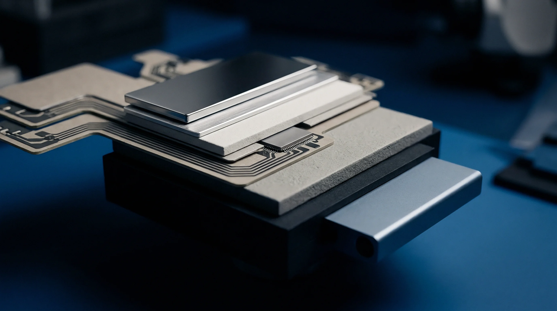
Physical removal of the protective plastic or ceramic packaging of an integrated circuit exposes the silicon die for direct inspection. This process of die decapsulation is necessary to analyze internal failures or verify the authenticity of electronic components. It must be performed with precision to avoid damaging the active circuitry.
Failure Analysis
Chemical solvents are used to dissolve the mold compound without affecting the internal bond wires or the silicon surface. This phase of die decapsulation uses fuming nitric acid or sulfuric acid at elevated temperatures to expose the silicon die. Technicians monitor the reaction closely to prevent over-etching of the aluminum pads, ensuring that the original electrical faults remain intact for subsequent microprobe testing.
Package Type
Different packaging materials require distinct etching techniques to preserve the structural integrity of the sample. While plastic packages yield to acid mixtures, ceramic enclosures require mechanical milling or laser ablation before chemical exposure. The choice of technique depends on the chemistry of the encapsulant.
Analytical Method
Advanced imaging techniques like scanning electron microscopy inspect the exposed die for physical anomalies after the removal of the package. This step of die decapsulation enables engineers to detect counterfeit dies or locate the exact point of an electrical short circuit. This forensic examination provides the final proof in quality disputes.