Meaning
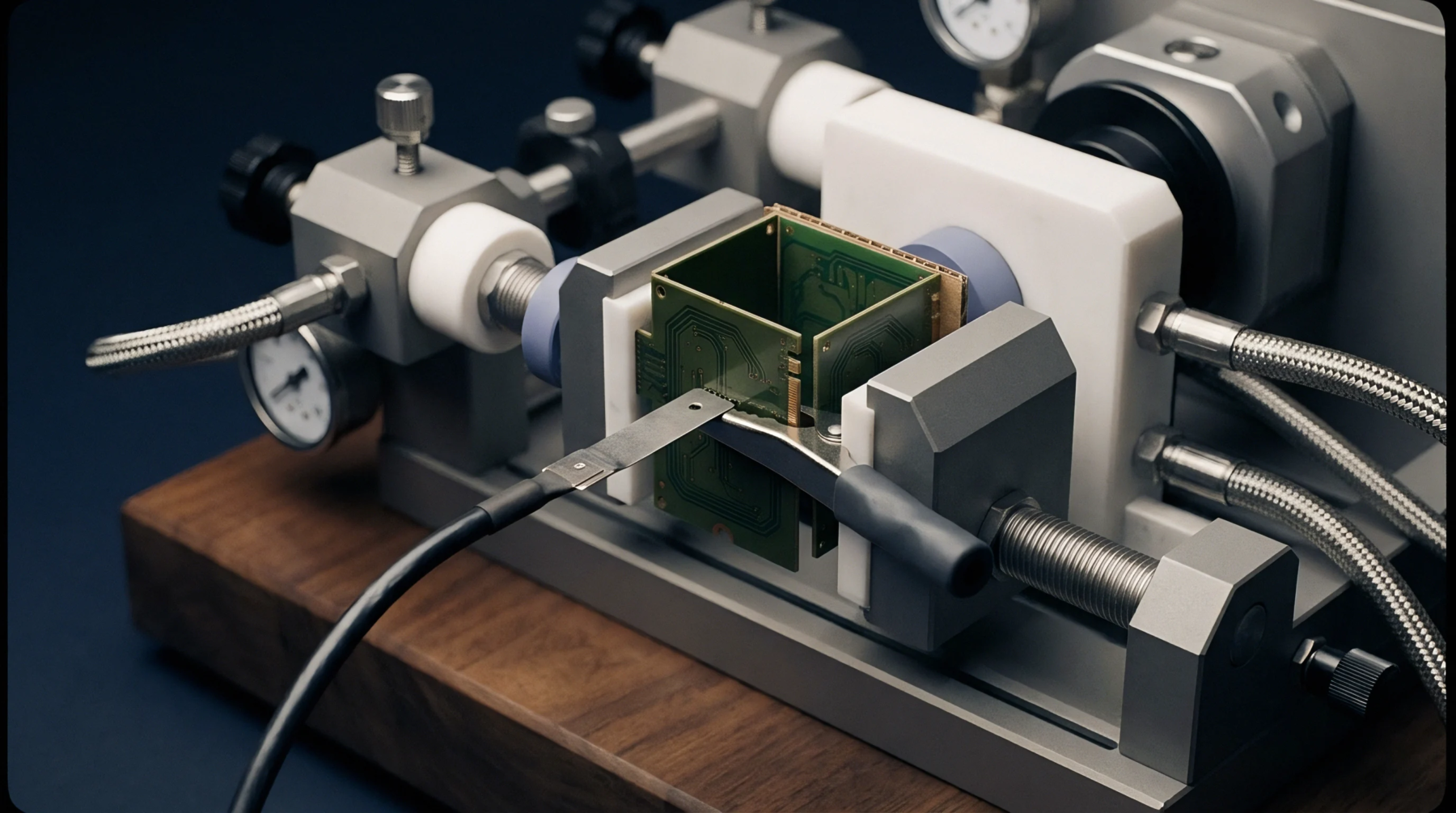
Parasitic electrical properties occur when conductive traces on different layers of a semiconductor die interact through a dielectric medium. Charge storage of this type directly influences the maximum switching frequency of the integrated circuit. The inter metal capacitance creates an unintended path for signal coupling.
Layer Separation
Increasing the thickness of the insulating material between metal tiers reduces the charge accumulation. The inter metal capacitance depends on the dielectric constant of the material and the vertical distance between conductors. Modern fabrication processes use specialized materials to minimize these parasitic effects in high-density designs.
Signal Crosstalk
Rapid voltage changes on one trace induce currents in neighboring lines through the electric field. High inter metal capacitance worsens the interference between clock signals and sensitive data paths. Designers mitigate this by placing grounded shields between critical routing layers to terminate the field lines.
Extraction Model
Precise calculation of these parasitic values is necessary for accurate timing simulation. The inter metal capacitance is modeled using three-dimensional field solvers that account for the complex geometry of the interconnect stack. Failure to include these values leads to timing violations where signals arrive too late for the capture clock edge.
Software tools extract these parameters from the physical layout files to provide a realistic view of circuit performance before the silicon is manufactured.