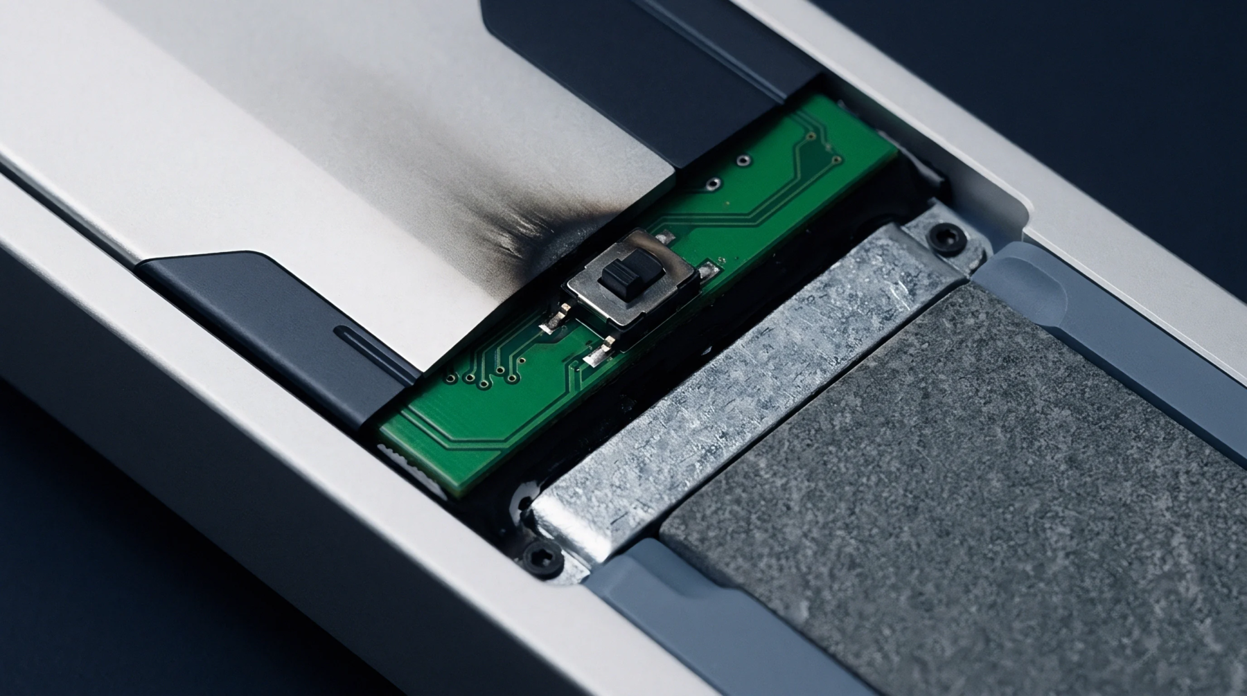
Meaning
Microscopic fractures within the dielectric layers of a printed circuit board are caused by mechanical stress or thermal cycles. This substrate micro-cracking disrupts the integrity of internal conductor vias and signal traces, leading to intermittent failures. It represents a physical breakdown of the fiberglass-epoxy matrix inside a multi-layer board assembly.
Stress Trigger
Thermal cycling of high-power chips creates high internal stresses due to mismatched expansion rates between materials. This physical generator of substrate micro-cracking is triggered by rapid temperature changes during operation. The stress accumulates at the corners of through-hole vias where copper meets resin.
Diagnostic Protocol
Board testing teams use electrical resistance testing and scanning electron microscopy to identify these hidden internal faults. To detect substrate micro-cracking, multi-layer circuit boards are subjected to thermal shock testing while continuously monitoring trace line impedance. A sudden spike in resistance indicates a fracturing event that is otherwise invisible to the naked eye.
This thermal cycling test ensures that only boards with structurally sound internal matrices are approved for final product integration, protecting the device from field failures.
Prevention Design
Flexible dielectric resins and balanced copper distribution reduce internal mechanical stress. For substrate micro-cracking, using epoxy resins with higher transition temperatures provides stronger support. This prevents flexing under thermal load.