Sub Terahertz Waveguide Interface Passive Intermodulation Characterization
Sub-terahertz waveguide interface passive intermodulation stems from oxide tunneling and micro-asperity non-linearities, mitigated by precise flange torque.
Hollow metallic transmission lines with nominal internal aperture dimensions of twenty-two thousandths of an inch by eleven thousandths of an inch guide electromagnetic waves throughout the sub-terahertz spectrum. Transceiver modules incorporate WR-2.2 waveguide channels to route radio frequency signals within the frequency band extending from three hundred twenty-five gigahertz to five hundred gigahertz. The rectangular metallic duct supports the fundamental transverse electric one-zero mode while attenuating out-of-band energy below its lower physical cutoff frequency near two hundred sixty-eight gigahertz.
The electrical applicability of this medium ceases when operating frequencies exceed five hundred gigahertz, where higher-order electromagnetic propagation modes trigger signal distortion and severe dispersion.
Signal loss inside the wave conduit scales sharply with increasing frequency due to electromagnetic skin effect losses occurring across the interior copper boundaries. Current travels within a skin depth measuring under one hundred nanometres at four hundred gigahertz, making internal wall surface roughness a primary driver of attenuation. Attenuation values frequently exceed fifteen decibels per metre in commercial gold-plated or silver-plated conduits, forcing system designers to minimize physical waveguide track lengths between active amplifiers and antenna apertures.
Because planar transmission lines exhibit prohibitive losses at these sub-terahertz frequencies, WR-2.2 waveguide remains the practical mechanism for low-loss power distribution inside ultra-high-frequency test fixtures and sensors.
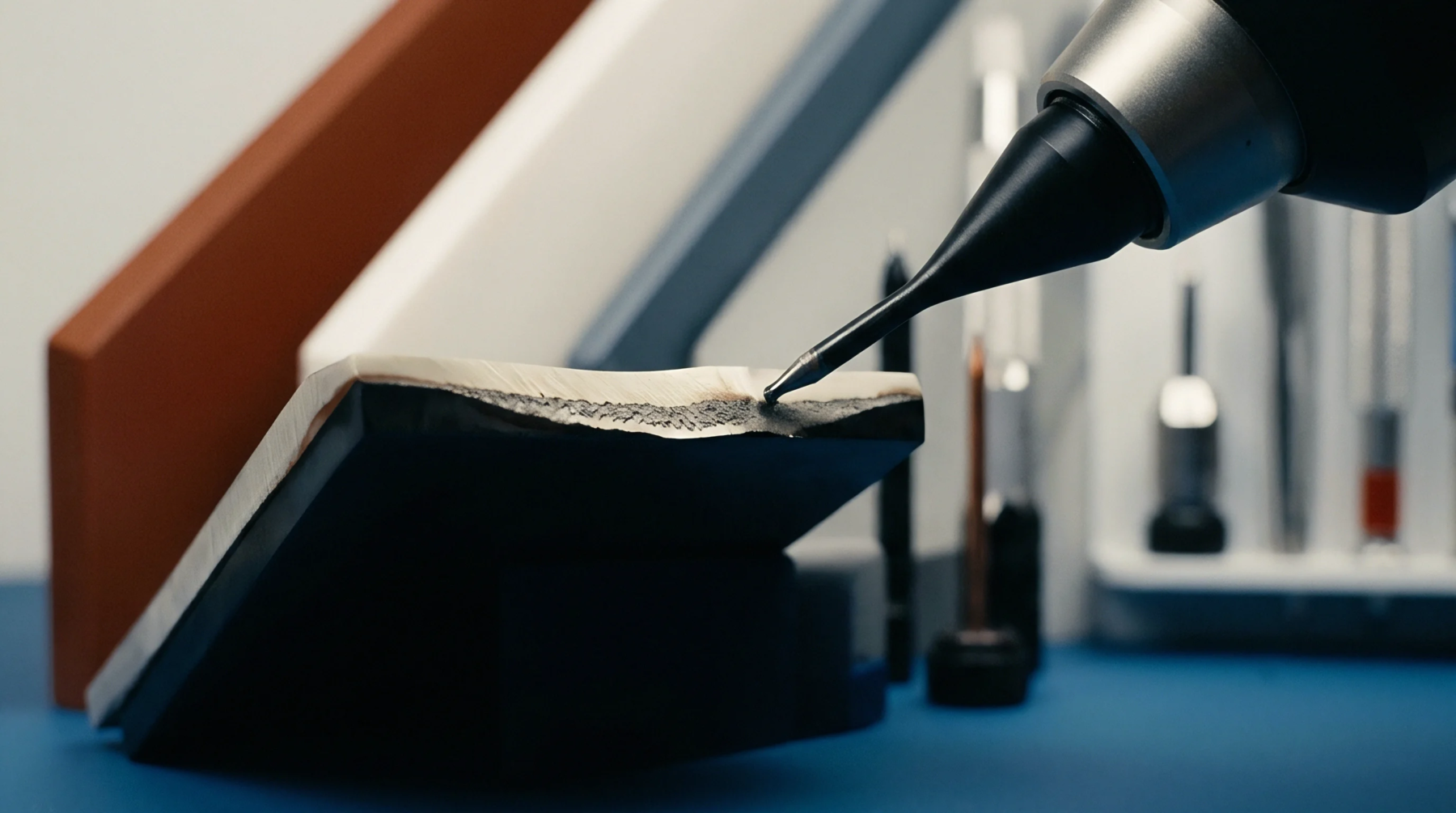
Manufacturing these tiny rectangular channels requires specialized machining technologies capable of sustaining tolerances tighter than two micrometres. Facilities employ split-block milling using micro-endmills under temperature-controlled cleanroom conditions, splitting the waveguide along the centreline of its broad wall to minimize transverse current disruption across the assembly seam. Alternative fabrication methods utilize silicon deep reactive ion etching followed by gold sputtering to build light, ultra-precise waveguide conduits for airborne applications.
When assembling split blocks, technicians inspect the mating faces using optical microscopy to guarantee that no microscopic burrs, foreign particulates, or plating blisters deform the interior WR-2.2 waveguide cavity.
Production test technicians confirm the operational integrity of waveguide components by measuring broadband S-parameters using vector network analyzers equipped with millimeter-wave frequency extension heads. Calibration routines demand specialized calibration kits containing matched loads, precision offset shorts, and flush thru connections aligned via IEEE 1785 or UG-387 flange hardware. Test certificates record insertion loss curves, port return loss values, and group delay stability across the entire three-hundred-twenty-five to five-hundred-gigahertz sweep.
Components passing these rigorous laboratory screenings earn final qualification stamps, certifying that the WR-2.2 waveguide delivers predictable sub-terahertz RF performance in scientific sensing and next-generation communications hardware.
Sub-terahertz waveguide interface passive intermodulation stems from oxide tunneling and micro-asperity non-linearities, mitigated by precise flange torque.
Expertise is a utility, not a secret. sentiention™ publishes its working knowledge as open reference: intelligence layer covering the materials it sources, the markets it enters, and the reference that serves both.