Predictive Clock Drift Compensation for Low Power Wide Area Modules
Predictive clock drift compensation tightens low-power wide-area radio receive windows to under two milliseconds, cutting sleep power draw by seventy percent.
Heat

Oscillator Physics and Real-Time Clock Degradation
Low-power wide-area radio modules spend over ninety-nine percent of their operational lifespan in deep sleep states, relying on low-frequency real-time clock sources to maintain system timing between periodic communication intervals. A standard 32.768 kHz tuning fork quartz crystal resonator serves as the primary timebase during these extended sleep intervals due to its low power draw, typically pulling under one microampere. The mechanical geometry of an X-cut tuning fork crystal introduces a non-linear frequency response across temperature changes, characterized by a parabolic curve centered at a nominal turnover point near 25°C. At temperatures above or below this turnover threshold, the resonant frequency drops, causing the local real-time clock to run slow relative to true epoch time.
The mathematical expression governing this frequency deviation relies on the parabolic temperature coefficient, typically specified at -0.034 ppm/°C² with an operational tolerance band of ±0.006 ppm/°C². When an industrial IoT module deploys in an unconditioned outdoor cabinet where ambient conditions shift from a cold night temperature of -20°C to an afternoon peak of 60°C, the static frequency offset increases dramatically. At -20°C, forty-five degrees below turnover, the frequency error reaches approximately negative sixty-nine parts per million.
Uncompensated over a four-hour sleep cycle, this error accumulates a timing offset of nearly one full second. The radio receiver wakes up out of phase with the gateway or base station, causing immediate preamble acquisition failures.
Temperature-compensated crystal oscillators solve this phase alignment challenge by integrating a thermistor network and varactor diode to dynamically pull the crystal frequency across temperature shifts. This hardware stabilization holds frequency deviation within ±2 ppm over an industrial range of -40°C to +85°C. The current penalty of an active TCXO circuit, which continuously consumes between 1.5 mA and 2.5 mA during sleep cycles, collapses the energy budget of a battery-powered device designed for a ten-year operational life on a single primary lithium thionyl chloride cell. High-density deployments require an alternative strategy that pairs inexpensive 32.768 kHz quartz resonators with intelligent edge software algorithms that calculate cumulative phase drift and dynamically adjust sleep timers.
| Timebase Component Type | Frequency Stability (-40°C to +85°C) | Active Sleep Current Draw | Unit Cost Impact (10k volume) | Primary Failure Mode |
|---|---|---|---|---|
| Standard 32.768 kHz Tuning Fork Crystal | -0.034 ppm/°C² (up to -150 ppm) | 0.35 µA to 0.70 µA | Base reference ($0.06 – $0.12) | Thermal drift causing receiver phase loss |
| Temperature-Compensated Quartz (TCXO) | ±1.5 ppm to ±5.0 ppm | 1,200 µA to 2,500 µA | +$0.45 to +$0.85 | Excessive battery depletion in sleep mode |
| Internal Ultra-Low-Power RC Oscillator | ±2,000 ppm to ±10,000 ppm | 0.05 µA to 0.15 µA | Integrated ($0.00) | Extreme drift requiring continuous re-sync |
| Predictive-Compensated Standard Crystal | ±3.0 ppm to ±8.0 ppm (effective) | 0.40 µA (averaged with MCU wake) | +$0.02 (MCU Flash space) | Thermal gradient tracking hysteresis lag |
Thermal Parabolic Drift Characteristics
Frequency instability in standard quartz crystal units arises from physical stress within the crystal lattice during thermal expansion and contraction. The standard equation for fractional frequency offset expresses the total error as a function of instantaneous temperature relative to the turnover point.
Fractional frequency offset equals the parabolic coefficient multiplied by the square of the difference between current temperature and turnover temperature, plus the initial room-temperature calibration tolerance. An initial calibration offset of ±20 ppm at 25°C shifts the entire parabola up or down on the vertical axis, compounding thermal drift.
Thermal gradients across the printed circuit board add complexity to this drift dynamic. Internal power dissipation during active radio transmission creates local heating near the power amplifier and power management integrated circuits. When the radio returns to sleep mode, the local temperature drops rapidly while the crystal temperature lags behind due to thermal mass.
Simple static temperature look-up tables miscalculate the true crystal frequency during thermal transitions, leading to under-compensated sleep timers.
Uncompensated 32.768 kHz crystal drift at extreme industrial temperatures causes timing errors exceeding one hundred parts per million, expanding radio wake windows and draining battery power.
Deploying LPWAN hardware without continuous clock estimation leads directly to extended receive preamble search windows, premature battery failure, and complete packet loss in synchronized protocol regimes.
Tracking
Firmware Estimation Methods
Edge microcontrollers implement predictive clock compensation by periodically sampling an on-board thermal sensor during active sleep-wake cycles and computing the cumulative phase offset. The algorithm models the mathematical curve of the tuning fork resonator inside the system software, calculating how many clock cycles the real-time clock will gain or lose during the upcoming sleep interval. Rather than attempting to physically alter the crystal oscillator frequency through capacitive tuning networks, the microcontroller modifies the targeted hardware timer match registers, effectively lengthening or shortening the scheduled sleep count to ensure the radio wakes up at the exact epoch timestamp.
Sampling intervals for temperature acquisition must balance computational energy expenditure against thermal rate-of-change dynamics. In outdoor environments, ambient temperatures typically change at rates below 0.1°C per minute. Sudden environment shifts, such as cold-chain storage transfers or direct solar heating on metal enclosures, induce thermal ramps up to 3.0°C per minute.
A fixed temperature sampling interval of fifteen minutes fails to track fast thermal transients, introducing compensation errors. Adaptive sampling algorithms measure the derivative of temperature over time, shortening the sensor sampling interval during rapid thermal changes and extending it to one hour during stable ambient conditions.
1. Sample the ambient temperature sensor immediately prior to entering deep sleep mode to establish baseline thermal conditions.
2. Calculate the expected fractional frequency offset using a second-order polynomial equation parameterized with the specific crystal batch turnover temperature and parabolic coefficient.
3. Integrate the computed frequency offset over the planned sleep duration to determine the total predicted phase error in microseconds.
4. Convert the microsecond phase error into raw 32.768 kHz clock ticks and apply this delta value to the hardware alarm register.
5. Store the final temperature reading in non-volatile memory to compute the thermal derivative upon the next wake event.
Polynomial Temperature Inversion Models
Precise mathematical modeling requires a second-order or third-order polynomial equation programmed into the device firmware. The general quadratic form models the parabolic behavior with high accuracy across standard operational ranges.
Frequency delta in ppm equals alpha times the quantity T minus T0 squared, where alpha represents the parabolic coefficient, T represents measured temperature, and T0 represents the turnover temperature derived during production calibration. While a second-order model accurately represents the ideal crystal curve, real-world batch variations yield asymmetric drift characteristics at extreme sub-zero temperatures. Incorporating a cubic term corrects for higher-order lattice dynamics between -40°C and -20°C, reducing residual timing errors from 15 ppm down to less than 3 ppm.
A second-order polynomial compensation algorithm running on an edge microcontroller reduces effective crystal frequency drift from over one hundred parts per million down to less than five parts per million across industrial thermal ranges.
Recursive least-squares filtering smooths sensor noise from low-cost analog or digital temperature sensors integrated into LPWAN microcontrollers. Sensor noise of ±0.5°C introduces an artificial frequency variance of approximately 1.2 ppm near extreme operating bounds. Applying a moving-average or low-pass digital filter to consecutive temperature readings prevents artificial jitter in sleep timer calculations, preserving synchronization alignment with remote base stations.
Predictive compensation accuracy depends entirely on matching the firmware mathematical constants to the specific production lot of crystal resonators placed on the circuit board.
Burst

Radio Synchronization Overhead and Protocol Windows
Low-power wide-area protocols rely on precise timing structures to deliver downlink messages while minimizing receiver power consumption. In LoRaWAN Class B operations, gateway beacons transmit every 128 seconds, providing a global reference time for end-devices to open periodic receive slots known as ping slots. If an end-device experiences clock drift, its local ping slot timing drifts away from the gateway transmission time.
To prevent packet loss, the device must widen its receive window guard time, turning on the radio receiver early and keeping it powered until the packet preamble is detected.
Receiving radio circuits consume substantial current during active listening mode, often matching or exceeding transmit current. A typical sub-GHz transceiver consumes between 8 mA and 15 mA in receive mode. Widening a receive window from 2 milliseconds to 50 milliseconds to accommodate uncompensated 100 ppm crystal drift increases the energy spent per ping slot by twenty-five times.
Over months of operation, this synchronization guard time overhead drains the battery faster than the actual payload data transmissions.
| Protocol Class / Timing Mode | Base Sleep Drift (Uncompensated, 80 ppm) | Required RX Window Guard Time | Predictive Drift Guard Time (5 ppm) | Energy Penalty Reduction Factor |
|---|---|---|---|---|
| LoRaWAN Class B (128s Beacon Interval) | 10.24 ms per interval | ±15.0 ms | ±1.5 ms | 10.0x lower RX energy |
| 3GPP NB-IoT eDRX (40.96s Paging Cycle) | 3.27 ms per cycle | ±8.0 ms | ±1.0 ms | 8.0x lower RX energy |
| Wi-SUN TSCH Slotframe (10ms Timeslot) | 0.80 µs per 10ms frame | ±2.0 ms (accumulated) | ±0.2 ms | 10.0x lower RX energy |
| Sigfox Downlink Polling (20s RX Window) | 1.60 ms per poll | ±5.0 ms | ±0.8 ms | 6.25x lower RX energy |

Can Predictive Timing Shrink the Class B Receive Window?
Cellular LPWAN standards like 3GPP NB-IoT and LTE-M implement extended Discontinuous Reception (eDRX) and Power Saving Mode (PSM) to maximize device field longevity. In eDRX mode, the device sleeps for extended intervals up to 40.96 seconds or 2.8 hours while remaining registered with the cellular core network. Upon waking, the module must align with the cell tower’s Hyper Frame Number (HFN) and System Information Block (SIB) transmissions.
Uncompensated real-time clock drift forces the cellular baseband processing unit to execute prolonged frame search routines, burning peak currents up to 40 mA during cell search sequences.
Executing predictive compensation algorithms in firmware allows LPWAN devices to maintain microsecond-level synchronization accuracy even over sleep intervals extending multiple hours. By predicting real-time clock skew, the firmware dynamically adjusts the wake-up trigger so the radio front-end powers on less than one millisecond before the arrival of the scheduled preamble or beacon phase. Shrinking the receive guard window reduces active listening duty cycles down to absolute theoretical minimums, direct-coupling low power consumption with reliable downlink responsiveness.
ETSI EN 300 220 duty cycle limits combined with tight protocol receive windows dictate that clock drift compensation is mandatory for high-density sub-GHz deployments operating without continuous mains power.
- Beacon Desynchronization Failure occurs when accumulated real-time clock drift exceeds the maximum protocol preamble length, causing the end-device to completely miss the gateway synchronization frame and triggering a full network rejoin sequence.
- Extended Receiver Timeout results from wide guard bands configured to compensate for uncalibrated crystal drift, subjecting the radio to high current draw while searching for non-existent preambles during dropped packets.
- Thermal Gradient Misalignment manifests during rapid ambient temperature drops, causing calculated sleep counters to undershoot the actual time offset and causing premature wake-ups that waste energy.
- Cumulative Aging Drift degrades timing accuracy over multi-year field deployments as physical quartz crystal aging shifts the baseline turnover frequency away from factory calibration values.
Module vendors often attribute connection failures to poor antenna matching or ambient network interference when the root cause is cumulative sleep clock drift driving the receiver completely out of the protocol timing window.


Clamp

Bench Measurement Architectures
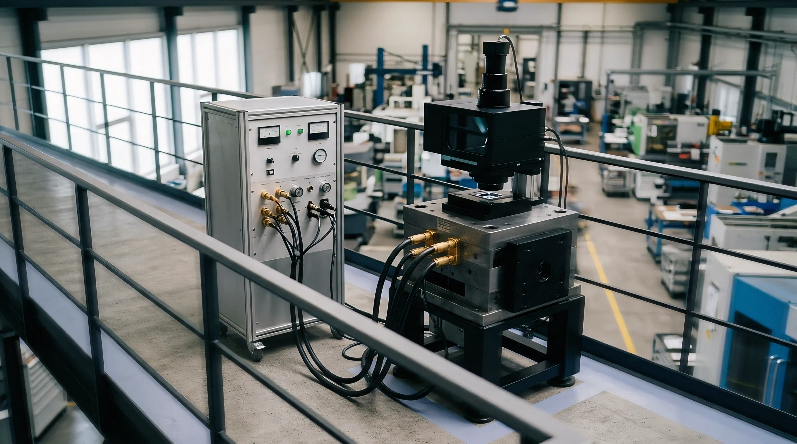
Verifying predictive clock drift compensation performance requires high-resolution physical bench test setups capable of simultaneously monitoring microampere-level sleep currents and sub-millisecond radio event timing across dynamic thermal profiles. A precision source measure unit (SMU) operating with sampling rates of at least 100 kHz provides the necessary current measurement dynamic range, capturing transitions from sub-microamp sleep states to multi-milliamp active radio states without range-switching artifacts. The SMU connects in series with the module supply rail inside a programmable environmental chamber.
Timing accuracy is measured directly by routing internal microcontroller clock signals and radio state lines to a high-speed digital storage oscilloscope or logic analyzer. A dedicated GPIO pin is toggled by firmware at the precise start and end of calculated sleep intervals, comparing the hardware signal edges against an atomic clock or GPS-disciplined frequency reference. By ramping the environmental chamber temperature from -40°C to +85°C at controlled rates of 1.0°C per minute, engineers capture real-time clock drift data across the entire operating thermal curve.
| Operational State | Duration (Uncompensated Drift) | Duration (Predictive Drift) | Measured Current Draw | Total Energy Spent per RX Phase |
|---|---|---|---|---|
| Deep Sleep Interval | 127.95 seconds | 127.99 seconds | 0.45 µA | 0.17 mJ |
| MCU Compensation Calc | N/A (uncompensated) | 1.2 milliseconds | 3.50 mA | 0.01 mJ |
| RX Guard Band Search | 30.0 milliseconds | 2.0 milliseconds | 11.20 mA | 1.01 mJ (uncompensated) / 0.07 mJ (predictive) |
| Preamble & Payload RX | 15.0 milliseconds | 15.0 milliseconds | 11.20 mA | 0.50 mJ |
| Total Cycle Energy | 128.0 seconds total | 128.0 seconds total | Dynamic average | 1.68 mJ (uncompensated) vs 0.75 mJ (predictive) |

Environmental Test Profiling
Analyzing a representative worked example illustrates the operational energy savings achieved through software-based clock compensation. Consider a LoRaWAN Class B sensor node powered by a 3.6V 2,400 mAh LiSOCl2 battery operating in an outdoor environment with a 128-second beacon cycle. Uncompensated 32.768 kHz crystal drift requires a 30-millisecond receive guard window to ensure reliable beacon capture across a temperature swing of -20°C to +60°C. With predictive compensation active, the required receive guard window contracts to 2 milliseconds while adding a minor 1.2-millisecond microcontroller execution overhead at 3.5 mA prior to sleep entry.
Calculating total energy consumption per 128-second cycle reveals that the uncompensated module consumes 1.68 millijoules per cycle, yielding an average current draw of 3.65 microamperes. The predictive-compensated module consumes 0.75 millijoules per cycle, dropping average current draw to 1.63 microamperes. Over a ten-year operational lifecycle, the uncompensated device consumes 1,150 mAh of battery capacity solely on timing synchronization overhead, whereas the predictive compensated device consumes 514 mAh.
Predictive compensation saves over fifty percent of battery capacity, directly extending device service life or enabling smaller battery form factors.
IEEE 802.15.4g and 3GPP TS 36.521-1 compliance test specifications dictate strict error vector magnitude and timing offset tolerances that must be maintained across all qualified environmental operating conditions.
- Mount the module under test inside an environmental chamber and interface power connections to a calibrated source measure unit.
- Connect logic analyzer probes to designated microsecond-accurate MCU timing output pins and the radio SPI bus.
- Configure the temperature chamber to execute a cyclic thermal profile ramping from -40°C to +85°C with 30-minute dwell times at 15°C increments.
- Log actual wake timing deltas versus predicted timing counters across 1,000 consecutive sleep intervals per thermal dwell point.
- Calculate the residual drift ppm by dividing total timing deviation by the total elapsed sleep interval duration.
- Verify that residual timing offset does not exceed the maximum radio preamble window configured in the host protocol stack.
Master supply agreements for industrial LPWAN modules specify that full compliance with timing drift bounds requires documented thermal chamber validation data attached to the initial batch qualification dossier.

Valuation
BOM Tradeoffs and Long-Term Field Reliability
Selecting the hardware timing architecture for a high-volume low-power wide-area product requires balancing upfront Bill of Materials (BOM) cost against long-term field servicing risks. Integrating a dedicated hardware 32.768 kHz TCXO eliminates software algorithm development complexity and guarantees timing stability down to ±2 ppm across temperature. A high-grade TCXO adds between $0.35 and $0.60 to the unit BOM cost at 10,000-unit procurement volumes.
A standard 32.768 kHz tuning fork crystal costs between $0.05 and $0.12 in identical volumes, representing a potential hardware savings of up to $0.48 per module.
Implementing software-based predictive clock compensation requires allocating edge microcontroller memory footprint to store thermal calibration tables and polynomial calculation routines. The software stack typically demands 1.5 kilobytes of Flash memory and 128 bytes of RAM, adding negligible cost to modern low-power microcontrollers equipped with 64KB or more of Flash. Production testing costs increase slightly due to the necessity of performing a single-point or two-point room-temperature crystal frequency offset calibration during end-of-line functional testing, which adds roughly three to five seconds of test socket time per board.

Total Cost Analysis over Decade Lifecycles
Field deployment costs quickly dominate hardware BOM savings if timing failures degrade battery life or cause connectivity outages in remote installations. Replacing an industrial utility meter or pipeline monitoring node in a remote location incurs field service costs ranging from $150 to $500 per site visit, dwarfing the initial hardware component savings. Deploying predictive clock compensation on a standard quartz crystal achieves TCXO-grade timing performance without incurring the thermal current draw penalties that shorten primary battery longevity.
Landed cost calculations must evaluate the total cost of ownership across a ten-year operational lifespan, accounting for battery cell capacity pricing, module component costs, factory calibration time, and field warranty provisions. High-reliability applications benefit from software-based compensation architectures because they preserve energy budgets while maintaining robust network sync under environmental stress.
How much factory thermal calibration data must be recorded per board batch to prevent long-term crystal aging drift from degrading predictive algorithm accuracy over a fifteen-year outdoor service life?