Quantifying Sleep Clock Phase Noise in Connected Systems
Quantifying 32.768 kHz sleep clock phase noise prevents active wake-up window widening and preserves multi-year battery budgets in low-power wireless nodes.
Phase
Oscillator Noise Mechanics in Duty-Cycled Radios
Clipping a current probe to a Bluetooth Low Energy module during sleep reveals a current draw that gradually expands. In duty-cycled transceivers, a 32.768 kHz reference clock sets the timing between active states. Wireless chipsets spend hundreds of milliseconds to several minutes in deep sleep, waking only to maintain network synchronization or send sensor payloads.
Static stability ratings in parts per million (ppm) cover long-term drift from temperature shifts and aging, but short-term phase instability directly dictates how accurately the receiver hits its wake-up window.
Phase noise is short-term, random fluctuation in an oscillator signal’s phase. On a spectrum analyzer, it shows up as sideband power surrounding the 32.768 kHz carrier fundamental. In the time domain, those same fluctuations translate directly into cycle-to-cycle and period jitter.
For a low-power node, timing jitter forces the receiver to open its window early to avoid clipping the incoming preamble. If phase noise widens that jitter margin, the receiver must turn on even earlier, running at peak active current longer before a packet ever arrives.
Integrating phase noise from 1 Hz to 100 Hz on a 32.768 kHz tuning fork crystal yields an RMS jitter of 12.4 nanoseconds at room temperature.
Close-In Spectral Density and Temporal Drift
Phase variations within 1 Hz to 100 Hz of the carrier shift individual clock edge arrivals. This close-in noise stems from flicker noise in the oscillator’s sustaining amplifier and structural resonances inside quartz or silicon MEMS resonators. Standard frequency counters average cycles across long gate times, hiding these rapid edge shifts.
As a result, a crystal rated at ±20 ppm static tolerance can generate short-term timing jitter that exceeds its calculated guardband during short sleep cycles.
Low-frequency phase noise hits energy budgets hard because receiver power states are heavily asymmetrical. A typical wireless SoC draws 1.2 microamps in deep sleep with the 32.768 kHz clock running, but jumps to 10.5 milliamperes the moment the radio wakes into receive mode. Static frequency offsets tell only half the story.
Every extra microsecond spent idling in active receive waiting for a preamble burns as much energy as thousands of sleep cycles. Unexpected sleep power draw often gets blamed on ambient thermal spikes when close-in sideband noise in the clock circuit is the real culprit.
Synthesis

Converting Spectral Phase Noise to RMS Jitter
Translating frequency-domain sideband power into time-domain pulse displacement requires integrating the single-sideband phase noise spectral density, L(f), over a target offset range. For a 32.768 kHz sleep clock in a duty-cycled radio, that critical range spans from 1 Hz up to half the timing engine’s sampling rate ~ typically capped at 100 Hz or 1 kHz.
Converting this integrated phase variance (in radians squared) through the carrier frequency yields root-mean-square (RMS) timing jitter in seconds. Close-in noise at 1 Hz and 10 Hz offsets dominates the total integrated jitter. Low-cost internal RC oscillators carry high flicker noise floors that produce far higher RMS jitter than quartz crystals, even when periodic calibration corrects their static frequency offset.
| Oscillator Type | Nominal Frequency Stability (ppm) | Phase Noise at 10 Hz Offset (dBc/Hz) | Integrated RMS Jitter (ns) | Recalibration Energy Penalty |
|---|---|---|---|---|
| 32.768 kHz AT-Cut Tuning Fork Crystal | ±20 | -85 | 12.4 | None (Continuous Passive Operation) |
| 32.768 kHz Ultra-Low-Power MEMS | ±50 | -72 | 45.8 | Low (Internal Temperature Bias) |
| Internal RC Oscillator (Uncalibrated) | ±250 | -48 | 310.2 | None (High Drift Overhead) |
| Internal RC Oscillator (Calibrated 10s Interval) | ±50 (Calibrated) | -52 | 185.5 | High (2.4 GHz Phase Locked Loop Wake-ups) |
| 32.768 kHz Temperature-Compensated TCXO | ±5 | -105 | 2.1 | Medium (Continuous Active Bias Circuitry) |
| Data measured at 25°C ambient temperature with nominal 3.3V supply voltage. RMS jitter integrated from 1 Hz to 100 Hz offset. Recalibration penalty accounts for high-frequency crystal and PLL active run time during calibration sequences. | ||||

Could Oscillator Jitter Mandate Continuous Recalibration Cycles?
Internal RC sleep oscillators save component count and board space, which makes them appealing for high-volume consumer designs. But correcting their low-frequency wander requires periodic alignment against a high-frequency crystal reference. To recalibrate an internal 32.768 kHz RC circuit, the wake-up controller has to spin up the main crystal oscillator (typically 16 MHz to 32 MHz) and run a hardware counter loop.
Microamps quickly compound into milliamperes.
Recalibration loops consume substantial active energy. Powering a 32 MHz main crystal and digital phase-locked loop for 2 milliseconds every 10 seconds creates an average current penalty that easily cancels out the sleep-current savings of dropping an external 32.768 kHz crystal. Rapid shifts in ambient temperature accelerate short-term phase noise, rendering fixed calibration intervals ineffective at preventing window overrun.
Whether dynamic temperature tracking algorithms can manage flicker noise within tight sleep budgets remains unproven in long-term industrial deployments.
Clamp
Protocol Receiver Window Widening Formulas
Wireless standards accommodate timing uncertainty by keeping the receiver open longer than the baseline packet duration. The guard time equation, Δt_guard, combines master and slave clock inaccuracies over the sleep interval t_sleep. While standard protocol stacks derive guard bands purely from static tolerance values, phase noise adds short-term jitter that demands extra timing margin on top of those calculations.
In Bluetooth Low Energy networks, connection events depend on strict anchor timing. The peripheral receiver powers up early by a guard offset: Δt_guard = (sleep_time) × (master_ppm + slave_ppm) + jitter_margin. If phase noise adds 50 microseconds of peak-to-peak jitter, the stack must expand Δt_guard to protect the link, leaving the RF front-end idling at peak current while listening to empty air before the master packet preamble arrives.
Bluetooth Core Specification 5.4 Clause 4.2.2 dictates receiver window widening based on combined master and slave sleep clock accuracy, directly scaling active Rx energy.
Cross-Protocol Guardband Dependencies
Low-power wireless specifications mandate strict safety margins for scheduled preamble searches, but timing failures take different forms depending on network topology and channel access rules.
- Preamble Search Misses occur when phase jitter pushes packet arrival outside the receiver’s listen window, forcing full-duty retry attempts.
- Connection Dropout Escalation forces Bluetooth Low Energy peripherals into high-power channel discovery loops after repeated timing misses.
- Time-Slotted Synchronization Loss in IEEE 802.15.4 TSCH networks breaks slot frame alignment, triggering rejoin sequences that pull tens of milliamperes.
- Paging Window Extension in LTE-M eDRX modes keeps the cellular modem RF front-end active across multiple frame boundaries while checking for paging indicators.
Battery life calculations usually assume nominal timing, but wireless protocols penalize nodes heavily when timing drifts. In LoRaWAN Class A devices, the node opens two receive windows (RX1 and RX2) at precise intervals ~ typically 1 and 2 seconds ~ after an uplink transmission. Phase noise in the sub-GHz sleep clock forces the node to open the RX1 window early.
If timing jitter causes the node to miss the downlink frame entirely, it retransmits the uplink at higher output power, compounding battery drain. Choosing an uncalibrated oscillator to save a few cents up front can drive the receiver into extended active listening, draining primary batteries years ahead of target lifespans.

Arithmetic
Worked Power Budget for a Ten-Second Duty Cycle
Evaluating the true impact of timing inaccuracy requires examining actual power figures over a multi-year operating period. Consider a sensor node powered by a 3.3 V, 225 mAh lithium primary cell, waking every 10 seconds to receive a control packet and send telemetry. The SoC draws 1.5 microamps in sleep, 12.0 milliamperes in receive, and 15.0 milliamperes for 2 milliseconds during transmission.
Under ideal zero-jitter conditions, the preamble requires an active receive window of 1.0 millisecond.
With a high-quality tuning fork crystal (-85 dBc/Hz phase noise at 10 Hz offset), integrated RMS jitter adds less than 1 microsecond of window extension. Thermal drift over temperature adds another 30 microseconds, bringing total active receive time to 1.03 milliseconds per 10-second cycle. Average receive current per cycle works out to 12.0 mA × (1.03 ms / 10,000 ms) = 1.236 microamps.
Adding sleep current (1.5 µA), receive overhead (1.236 µA), and transmit overhead (3.0 µA) yields a total average system current of 5.736 microamps. The 225 mAh battery lasts roughly 4.47 years.
| Clock Architecture | Base Sleep Current (µA) | Window Extension (µs) | Active Rx Current (mA) | Average System Current (µA) | Expected Battery Life (Years) |
|---|---|---|---|---|---|
| High-Q Crystal (Low Phase Noise) | 1.5 | 30 | 12.0 | 5.74 | 4.47 |
| Standard Tuning Fork Crystal | 1.5 | 120 | 12.0 | 5.84 | 4.39 |
| Internal RC Oscillator (High Phase Noise) | 1.2 | 850 | 12.0 | 6.72 | 3.82 |
| Internal RC Oscillator (Uncalibrated Drift) | 1.2 | 2400 | 12.0 | 8.58 | 2.99 |
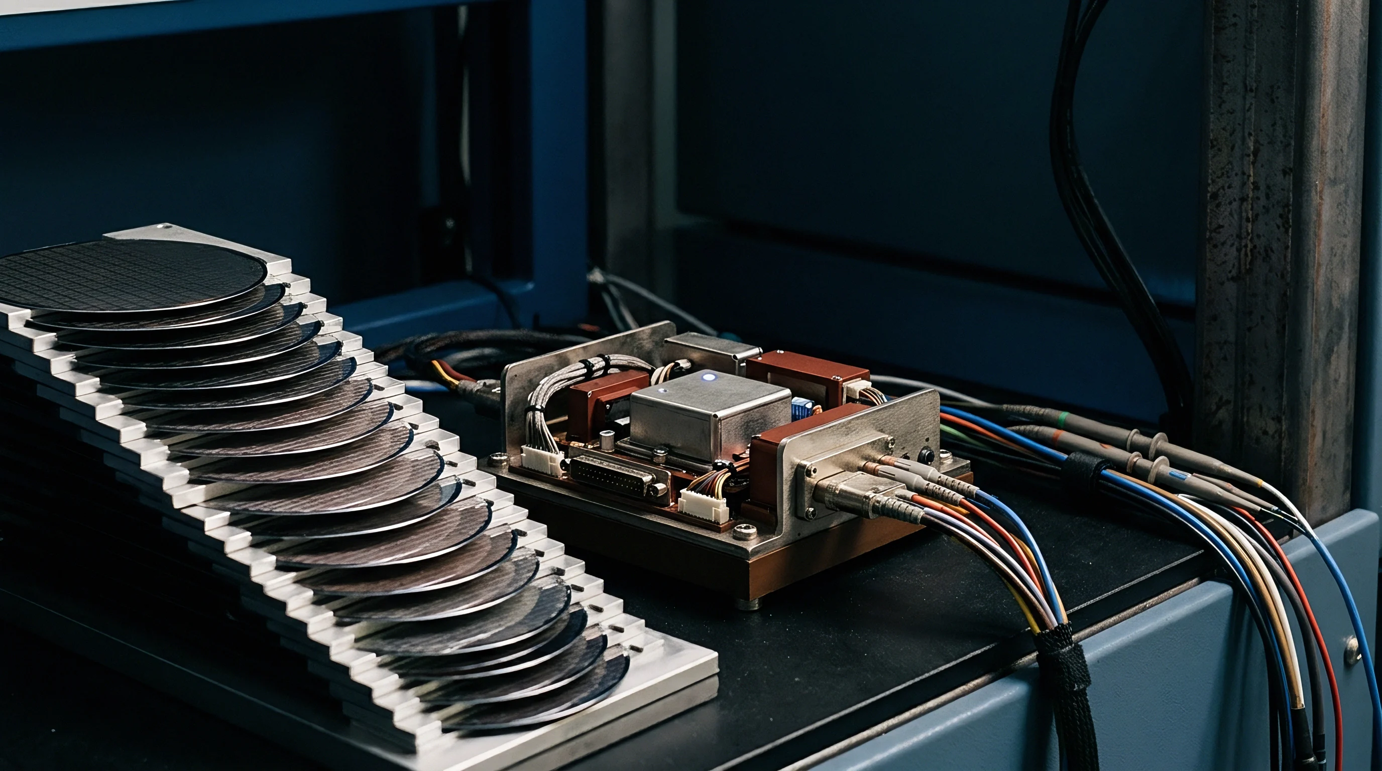
Quantifying Thermal and Aging Penalty Factors
Now substitute an ultra-low-cost internal RC oscillator into that same design. Close-in phase noise (-48 dBc/Hz at 10 Hz) combined with short-term thermal drift expands the required window extension to 850 microseconds. Total active receive time jumps from 1.03 milliseconds to 1.85 milliseconds, pushing average receive current draw to 12.0 mA × (1.85 ms / 10,000 ms) = 2.22 microamps.
Calculating the operational degradation caused by low-frequency clock noise follows a standard sequence:
- Measure close-in single-sideband phase noise power spectral density from 1 Hz to 100 Hz offset using a high-resolution signal source analyzer.
- Integrate sideband noise spectral density over the offset frequency band to calculate total phase variance in radians squared.
- Convert phase variance into time-domain root-mean-square jitter using the carrier frequency reference relationship.
- Add root-mean-square jitter to static parts-per-million frequency tolerance to determine total window widening time.
- Multiply active receiver current by calculated window extension duration to derive the energy penalty per sleep cycle.
Short-term timing jitter dictates receiver wake-up guardbands far more aggressively than static temperature drift over short sleep intervals.
That jump contracts device lifespan sharply. Average system current rises to 6.42 microamps, cutting cell life from 4.47 years to 4.00 years. If the internal RC oscillator experiences uncalibrated thermal drift, window extension reaches 2,400 microseconds ~ pushing average current to 8.28 microamps and dropping lifespan to 3.10 years.
Cheap timing components sacrifice over 30 percent of operating life. Relying strictly on static parts-per-million ratings guarantees that timing guardbands will burn more energy over the product’s life than the radio’s baseline sleep current.
Verification
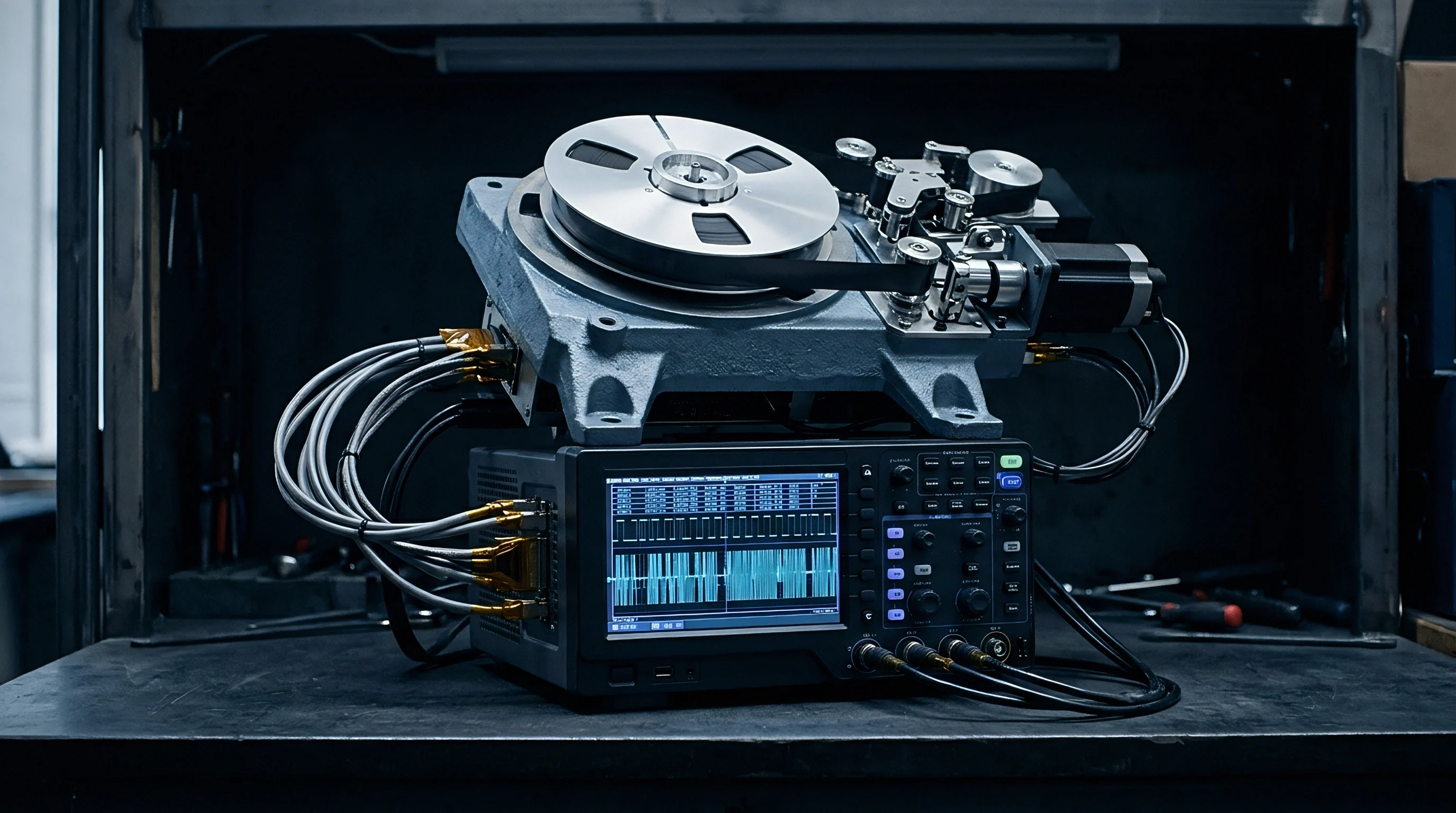
Bench Setup for Low-Frequency Spectral Measurements
Measuring sideband noise power within 10 Hz of a 32.768 kHz carrier poses real challenges on the bench. Standard RF spectrum analyzers lack the frequency resolution and low-frequency baseband capability to resolve close-in sidebands below 100 kHz. Engineers rely on dedicated Signal Source Analyzers (SSA) with cross-correlation engines, which lower the instrument’s internal noise floor enough to resolve phase noise down to -140 dBc/Hz at 10 Hz offset on low-amplitude 32.768 kHz signals.
Physical-layer probing must also minimize capacitive loading. Attaching a standard 10x passive probe (10 pF to 15 pF) directly to 32.768 kHz crystal pins detunes the oscillator, distorting true phase noise behavior and altering startup margins. Active high-impedance FET probes (under 0.8 pF input capacitance) should be buffered through a unity-gain amplifier before feeding the analyzer input.
Qualification Protocols for Low-Power Crystal Selection
Evaluating alternative timing sources requires thermal ramps and supply voltage testing to surface phase instability before committing to volume BOMs.
- Low-Frequency Spectrum Analyzers with ultra-low noise floors capture close-in phase noise sidebands at 1 Hz and 10 Hz offsets from the 32.768 kHz carrier.
- High-Speed Logic Analyzers cross-triggered with dynamic current probes correlate microsecond-level timing offsets against transceiver current transitions.
- Thermal Chamber Ramps evaluate oscillator phase noise fluctuations across industrial ambient temperature ranges from -40°C to +85°C.
- Supply Voltage Sags simulate battery discharge curves to quantify phase noise variations as cell voltage decreases toward operational cutoffs.
Verification protocols must isolate close-in sideband noise from thermal frequency drift using cross-correlated spectral measurements.
When qualifying completed radio modules, engineers log continuous current traces across 72-hour test runs inside environmental chambers. Spikes in average current draw show where phase noise jitter broke past calculated guardbands, forcing the stack into retry routines. Specifying IEEE 802.15.4-2020 Clause 6.9.3 timing compliance in module procurement contracts ensures vendors guarantee jitter performance under active thermal ramping.

Ledger
BOM Cost Tradeoffs against Battery Longevity
Hardware economics balance component cost against long-term field support. A standard 32.768 kHz quartz tuning fork crystal adds roughly $0.04 to $0.08 to a high-volume BOM. Temperature-compensated crystal oscillators (TCXO) or low-jitter MEMS sources run between $0.25 and $0.45 per unit.
Sourcing managers often push to drop dedicated external crystals in favor of internal RC oscillators embedded in the SoC.
An internal RC oscillator cuts $0.05 in component costs and frees 4 square millimeters of board space. But the expanded wake-up windows quickly eat up those initial savings. On a commercial utility meter or asset tracker rated for 10 years, early battery depletion triggers manual technician visits.
With field service calls costing $75 to $250 per node in industrial settings, saving five cents on procurement creates massive risk over the product’s operational life.
Module suppliers frequently present sleep current under ideal crystal conditions while omitting the energy cost of periodic RC oscillator recalibration loops.
Regulatory and Carrier Acceptance Ramifications
Cellular IoT deployments specify maximum clock drift during extended discontinuous reception. Technologies such as LTE-M (eDRX) and NB-IoT (PSM) use sleep intervals spanning from seconds to multiple hours, and network operators strictly enforce paging window timing under 3GPP Release 13/14 standards. If an IoT module’s clock carries excessive phase jitter, the modem misses its scheduled Paging Indicator Channel (PICH) frame.
Missing a paging frame forces a full cell re-selection and random access procedure. Cellular re-attaches pull peak currents over 250 milliamperes for several seconds, destroying annual power budgets in moments. Carrier test labs will reject modules showing sleep clock phase instability during extended eDRX tests.
Procurement specs need clear phase noise limits over temperature to ensure carrier certification, rather than relying on component unit price alone.