Isolating Clock Harmonics in Multi-Radio Embedded Designs
Isolating clock harmonics requires unbroken ground reference planes, near-field probe pre-scanning, and compliance spot-checks prior to formal qualification.
Origin
Digital square waves generated by system oscillators transfer energy far beyond their fundamental operating frequency. Microcontrollers, application processors, and display drivers toggle clock lines with rise times frequently under one nanosecond. Fourier analysis of a periodic trapezoidal wave confirms that high-frequency spectral energy decays at 20 dB per decade up to the corner frequency set by rise time, above which attenuation steepens to 40 dB per decade.
Fast edge rates extend harmonic energy into the gigahertz spectrum. A 24 MHz system clock driving a memory interface produces its 100th harmonic at 2400 MHz, landing inside the primary passband of co-located 2.4 GHz Wi-Fi and Bluetooth transceivers.

Harmonic Generation across Microcontroller Clock Lines
Harmonic frequencies align with integer multiples of the fundamental clock rate. When a 52 MHz application processor clock operates adjacent to a Sub-1 GHz transceiver tuned to 884 MHz, the 17th harmonic falls directly into the receiver passband. The spectral width of these harmonic lines depends on clock jitter and frequency stability.
Crystal oscillators produce narrow spectral spikes that concentrate electromagnetic energy into tight frequency bins, creating localized peaks on a spectrum analyzer. These sharp peaks readily exceed regulatory limits during radiated emissions testing.
Coupling Paths into Co-Located Wireless Radios
Coupling occurs through three primary mechanisms: direct trace-to-antenna radiation, conducted noise through shared power distribution networks, and ground plane impedance coupling. When a high-speed clock trace runs across an interrupted ground plane, the return current loops around the slot, forming an efficient loop antenna. This loop converts differential-mode clock currents into common-mode noise that propagates across internal cabling and PCB edges.
Power supply rails serving both digital processors and radio frequency integrated circuits act as direct conduction channels. Clock noise riding on power lines modulates the radio local oscillator or passes directly into the low-noise amplifier, degrading receiver sensitivity.
| Clock Frequency (MHz) | Harmonic Order | Target Harmonic Frequency (MHz) | Affected Wireless Service | Primary Coupling Mechanism |
|---|---|---|---|---|
| 24.00 | 100 | 2400.00 | Bluetooth / 2.4 GHz Wi-Fi | Radiated trace coupling to chip antenna |
| 38.40 | 24 | 921.60 | Sub-1 GHz ISM / LoRa | Power distribution network common-mode noise |
| 48.00 | 50 | 2400.00 | IEEE 802.15.4 / Zigbee | Ground bounce excitation of board ground plane |
| 52.00 | 17 | 884.00 | Sub-1 GHz LoRaWAN | Differential loop current from clock line slot |
| 100.00 | 52 | 5200.00 | 5 GHz Wi-Fi (UNII-1) | Direct radiation from unshielded memory bus |
Whether internal integrated circuit substrate isolation can suppress sub-harmonic phase noise before it reaches the low-noise amplifier remains an open engineering question.

Trace
Isolating clock-generated noise from transmitter spurious emissions demands dynamic spectrum analysis during active RF operation. Diagnostic pre-compliance scanning separates digital clock harmonics from RF synthesizer spurious emissions. Spectrum analyzers connected to magnetic near-field probes pick up localized electromagnetic fields directly above microcontroller ICs, clock buffers, and microstrip lines.
Setting the resolution bandwidth according to standard compliance specifications yields accurate amplitude capture: 120 kHz for measurements between 30 MHz and 1 GHz, and 1 MHz for frequencies above 1 GHz.
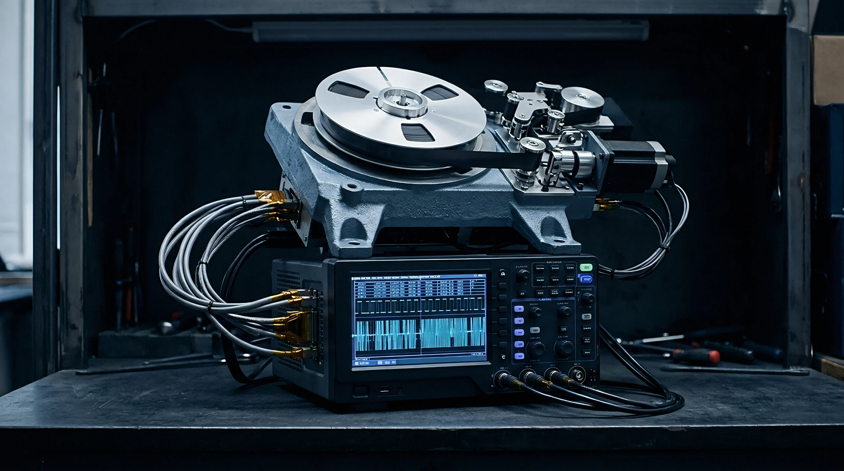
Diagnostic Bench Workflows and Probe Techniques
Identifying the precise source of a spurious emission calls for observing spectral behavior under varying operational states. Altering the transceiver channel frequency delivers immediate diagnostic clarity. When the RF carrier shifts from 2412 MHz to 2437 MHz, synthesizer-generated spurs move proportionally across the display.
Clock harmonics remain rigidly fixed at integer multiples of the host clock crystal.
Radiated field strength drops by 6 dB per doubling of distance when measured beyond the near-field boundary of a 100 MHz clock trace.
- Slot reference breaches create loop antennas where high-speed clock traces cross ground plane splits, elevating radiated emissions by up to 20 dB.
- Unfiltered power taps allow clock harmonics to ripple into transceiver voltage supply lines, inducing phase jitter on synthesized RF output carriers.
- Exposed clock stubs act as quarter-wave resonant structures at microwave frequencies, projecting high-energy harmonic spikes directly into internal radio antennas.
- Via transition discontinuities force clock return currents onto adjacent power planes, converting differential signals into broad common-mode noise across the board layout.
Chamber Isolation and Turntable Discrimination
Full-compliance radiated spurious measurements take place in a 3-meter semi-anechoic chamber. The device under test sits on a motorized turntable rotating through 360 degrees while the receiving antenna scans from 1 to 4 meters in height. Polarizations shift between vertical and horizontal alignment to capture maximum field strength.
In testing conducted under CISPR 16-1-1 guidelines using a peak detector with a 120 kHz resolution bandwidth at 3 meters, a 48 MHz clock harmonic measured 44.2 dBuV/m at 480 MHz. This specific measurement rests on a calibrated bilogical antenna setup with 2.1 dB measurement uncertainty, and increasing the ground plane perimeter stitching from 10 mm to 3 mm drops this emission to 36.5 dBuV/m.
Clock harmonics always remain stationary on the spectrum display when the operating channel of the co-located transceiver is shifted.


Shield
Physical suppression of high-frequency clock currents relies on controlling the return current loop area on internal circuit board layers. High-speed clock layout relies on unbroken ground reference planes on adjacent inner PCB layers. Routing a clock line directly above a solid ground plane concentrates the return current directly beneath the signal trace, minimizing the loop area and reducing radiated electromagnetic fields.
Microstrip routing on surface layers emits higher radiated fields than stripline routing embedded between two continuous ground planes. Stripline structures deliver intrinsic attenuation for high-frequency clock harmonics.
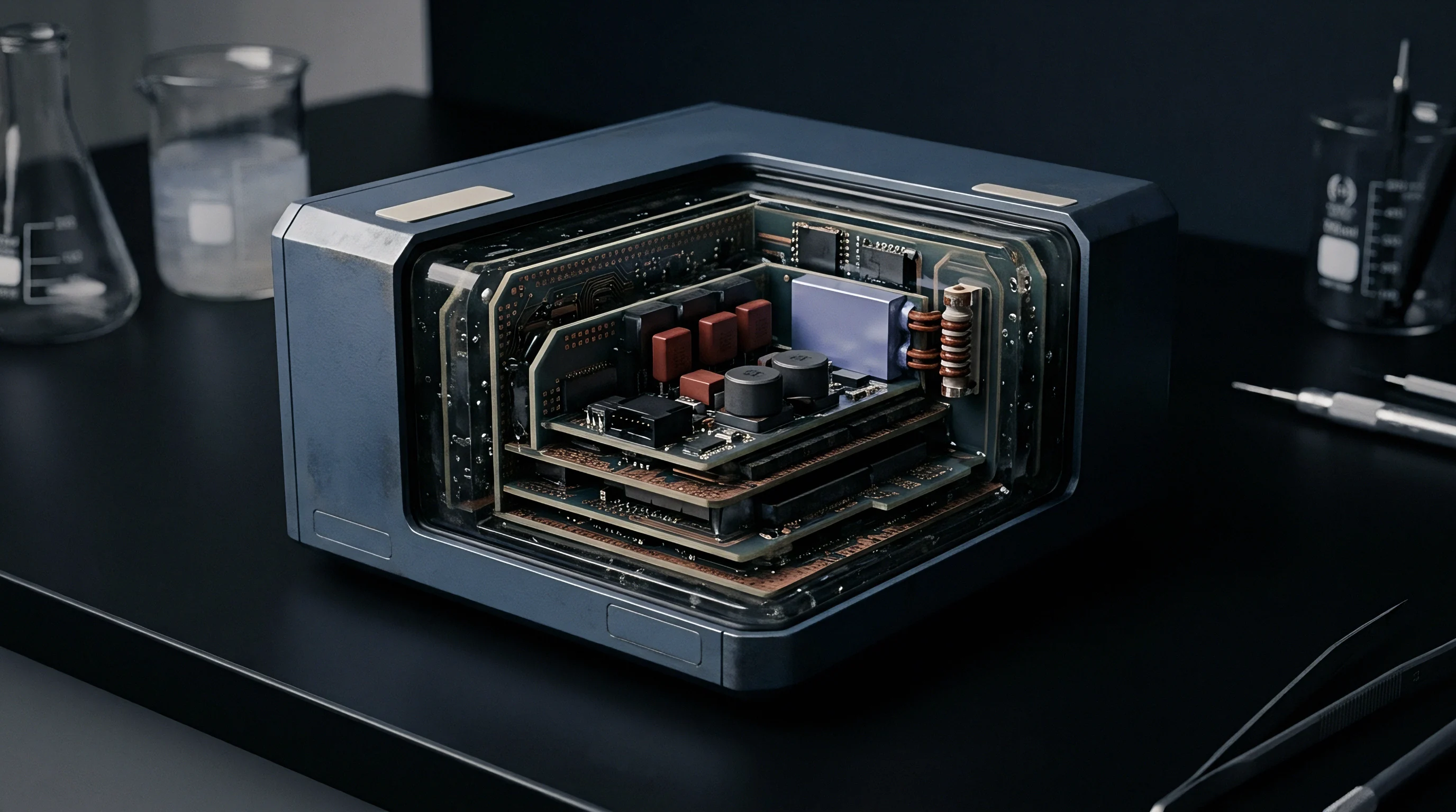
Board-Level Layout and Grounding Architectures
Stitching vias positioned along clock trace edges reinforce reference plane continuity. Spacing stitching vias closer than one-twentieth of the wavelength corresponding to the highest clock harmonic prevents electromagnetic leakage between ground layers, while ferrite beads on supply rails and shielding cans over noisy ICs absorb high-frequency energy and contain direct radiation. Placing a series damping resistor of 22 to 33 ohms adjacent to the clock driver output pin rounds off sharp signal switching edges, reducing high-order harmonic amplitudes without degrading digital signal integrity.
Stitching ground vias positioned along clock trace perimeters maintain reference plane continuity across high-speed signal layer transitions.
Spread-Spectrum Clocks and Passive Suppression
Spread-spectrum clock generation modulates the fundamental clock frequency by 0.5% to 1.5% using a triangular modulation profile. This technique spreads concentrated harmonic energy across a wider bandwidth, lowering peak amplitudes observed by CISPR quasi-peak and average detectors.
- Position series damping resistors within two millimeters of the clock driver output pins.
- Verify that clock signals route exclusively on internal stripline layers bounded by solid ground planes.
- Place stitching ground vias at maximum four-millimeter intervals along the entire run of high-speed clock traces.
- Install board-level shielding cans covering digital processing units and clock distribution networks.
- Insert ferrite beads with high impedance at 1 GHz on power supply lines feeding digital clock buffers.
| Suppression Technique | Implementation Target | Typical Attenuation (dB) | Primary Frequency Impact Range | Design Trade-Off |
|---|---|---|---|---|
| Stripline Embedded Routing | High-Speed Clock Traces | 12 to 18 dB | 300 MHz to 6 GHz | Increases layer count and PCB stackup cost |
| Series Damping Resistors (33 Ohm) | Clock Driver Outputs | 6 to 10 dB | High-order harmonics above 500 MHz | Slightly increases signal rise and fall times |
| Spread-Spectrum Clocking (1.0% Downspread) | System Oscillator Tree | 8 to 14 dB | All clock harmonics | Adds timing jitter to high-speed bus interfaces |
| Perimeter Ground Via Stitching | Board Edge and Split Boundaries | 10 to 15 dB | 30 MHz to 3 GHz | Requires additional board real estate for vias |
| Surface-Mount Shielding Can | Digital IC and Clock Buffers | 15 to 25 dB | 100 MHz to 10 GHz | Adds height profile and component sourcing line |
Inadequate ground plane stitching beneath a high-speed clock bus causes unshielded common-mode currents to excite the board chassis, driving radiated emissions past regulatory thresholds and forcing a full printed circuit board spin.

Filing
Regulatory submissions for multi-radio embedded hosts treat clock harmonics differently depending on whether emissions originate from unintentional logic circuits or intentional RF synthesis. Unintentional radiators fall under FCC Part 15 Subpart B in the United States and CISPR 32 in Europe. Class B digital device limits enforce maximum radiated emissions of 40 dBuV/m between 30 MHz and 88 MHz, scaling to 54 dBuV/m average for frequencies above 960 MHz measured at 3 meters.
When clock harmonics overlap active transceiver bands, regulatory scrutiny increases because spurious emissions must satisfy both digital device limits and intentional radiator out-of-band requirements.

Regulatory Limits across Global Markets
Under FCC Part 15.247 and Part 15.209, spurious emissions falling within restricted frequency bands adhere to general radiated emission limits. In Europe, ETSI EN 301 489-1 governs electromagnetic compatibility for radio equipment, mandating radiated spurious limits of -36 dBm up to 1 GHz and -30 dBm from 1 GHz to 12.75 GHz during active operation. Under ETSI EN 301 489-1 Clause 8.2, the radiated spurious limit of -36 dBm below 1 GHz rests on a 3-meter semi-anechoic measurement setup using a quasi-peak detector; changing to a peak detector with a fast sweep speed elevates the measured value by up to 4 dB, potentially pushing a marginal pass into a non-compliance finding.
ETSI EN 300 328 Clause 4.3.2.11 enforces receiver spurious emission thresholds of -57 dBm up to 1 GHz and -47 dBm above 1 GHz when the radio operates in receive mode.
Compliance with ETSI EN 301 489-1 Clause 8.2 restricts radiated spurious emissions to -36 dBm below 1 GHz during active transceiver operation.
Permissive Changes and Modular Approval Scope
Integrating a pre-certified radio module does not exempt host devices from spurious emission compliance, as host layout changes trigger re-evaluation. Under FCC KDB 996369 D04 guidance, host manufacturers execute radiated spot-checks to confirm that host clock noise does not degrade pre-approved module emissions. Minor layout modifications that maintain compliance without increasing recorded emission levels qualify as Class I Permissive Changes, calling for internal documentation only.
If host clock coupling increases radiated emissions beyond previously filed levels while staying under statutory limits, a Class II Permissive Change filing becomes necessary, demanding accredited laboratory test reports and formal Telecommunications Certification Body submission.
- Module grant condition verification confirms whether the modular approval permits co-location with active host processing clocks without supplemental evaluation.
- Radiated spot-check testing determines if host clock harmonics elevate the composite device noise floor above modular baseline filings.
- Permissive change threshold review dictates whether observed emission increases require internal Class I record updates or formal Class II TCB submission.
- User manual standard disclosures enforce mandatory FCC Part 15 warning statements regarding co-location and unintentional radiator operation.
| Market Jurisdiction | Applicable Standard | Frequency Range | Statutory Limit Value | Enforcement Agency / Certification Route |
|---|---|---|---|---|
| United States | FCC Part 15 Subpart B Class B | 30 MHz to 88 MHz | 40.0 dBuV/m at 3m (Quasi-Peak) | FCC / SDoC or TCB Grant |
| United States | FCC Part 15.209 / 15.247 | Above 960 MHz (Restricted) | 54.0 dBuV/m at 3m (Average) | FCC / TCB Formal Grant |
| European Union | ETSI EN 301 489-1 / EN 300 328 | 30 MHz to 1 GHz (Tx Active) | -36.0 dBm (approx 57.0 dBuV/m) | CE Marking / EU Declaration of Conformity |
| European Union | ETSI EN 300 328 (Rx Mode) | 1 GHz to 12.75 GHz | -47.0 dBm (approx 48.0 dBuV/m) | CE Marking / Technical File Inspection |
| Japan | Radio Law Article 38-24 / Giteki | 30 MHz to 26 GHz | Technical Regulations Conformity | MIC / Registered Certification Body |
Inclusion of FCC KDB 996369 D04 Clause 3.2 in host assembly instructions shifts mandatory radiated spurious verification onto the integrator prior to commercial distribution.

Outlay
Financial reserves committed to radio certification collapse quickly when clock harmonic failures surface during final qualification testing. Booking an accredited 3-meter semi-anechoic chamber costs between $1,800 and $3,500 per 8-hour shift, excluding engineering support fees. Failing a radiated spurious emissions test during formal qualification halts the compliance sequence.
Resolving clock harmonic issues after board freeze introduces secondary costs that eclipse chamber hourly rates.
Test Chamber Economics and Retest Costs
Redesigning a multi-layer printed circuit board stackup to correct ground plane discontinuities or add clock filtering takes two to four weeks of layout time, $3,000 to $8,000 in fast-turn PCB fabrication fees, and two weeks of assembly and bench verification, consuming six weeks overall. Chamber rebooking delays typically range from three to six weeks depending on laboratory availability. Industry estimates for average laboratory retest waiting queues range from two to six weeks across regional test houses, making a two-week chamber slot reservation during initial contracting essential to mitigate potential retest delays.
Pre-compliance chamber testing completed prior to PCB artwork freeze prevents board respins that stall market launch schedules by two months.
Filing Timelines and Market Entry Arithmetic
A worked calculation demonstrates the economic impact of discovering clock harmonic compliance failures early versus late in the product development cycle.
Assume an industrial gateway incorporating a 100 MHz application processor clock and a pre-approved 2.4 GHz Wi-Fi module scheduled for release in the United States and the European Union.
In an early mitigation path, pre-compliance bench evaluation across two shifts totals $4,000, while adding series damping resistors and perimeter via stitching during initial layout adds $500 in engineering time. Initial formal qualification chamber testing under FCC Part 15B and ETSI EN 301 489 costs $12,000, passing on the first attempt. TCB review and CE technical dossier compilation total $3,500, yielding a cumulative outlay of $20,000 across a four-week lead time.
In a late failure path, initial qualification testing fails due to clock emissions at 400 MHz and 2400 MHz, sinking the initial $12,000 fee. Engineering diagnostic shifts consume $2,500, a four-layer PCB respin and fast-turn fabrication cost $6,500, and redesign labor adds $4,500 across 30 engineering hours. Formal re-testing in an accredited chamber adds $10,000, and TCB re-submission fees cost $2,000, driving total expenditure to $37,500 with a seven-week delay.
Certified transceivers bear no responsibility for clock harmonics generated by host processor traces routed outside the shielded module boundary.