Establishing Multi Component Integrated Circuit Tariff Eligibility under Chapter Note Rules
Establishing multi-component integrated circuit tariff eligibility under Chapter Note rules requires verifying single-package encapsulation, die count ratios, and discrete component boundaries through laboratory teardown data.
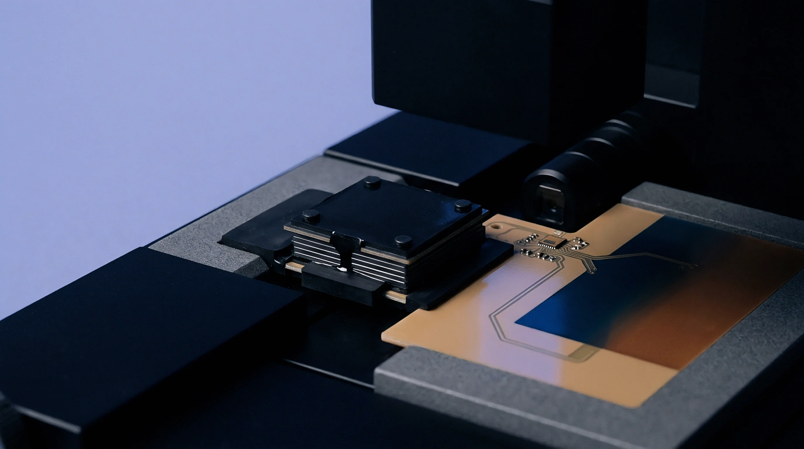

Silicon
Modern semiconductor packaging houses active micro-circuitry alongside discrete surface-mount components within a single resin shell. Wafer fabrication produces monolithic dies connected via wire bonds, copper pillars, or flip-chip bumps to a shared leadframe or organic substrate. This physical arrangement dictates whether customs conventions classify the finished package as a semiconductor device or an electrical assembly.

Die Combinations and Encapsulated Architecture
Integrated circuits inside a multi-component package must form a single, indivisible structural unit after resin transfer molding. High-density interconnect carriers can house microprocessor dies next to high-bandwidth memory stacks and radio-frequency transceiver units. Encapsulation establishes the package boundary, leaving terminal leads or ball grid arrays ready for surface mounting without further physical modification.
A multi-component integrated circuit housing three distinct semiconductor dies on an organic interposer retains structural unit status under international customs standards.
Integration requires every active chip to connect directly to the supporting interposer or leadframe. Multi-chip modules combining stacked storage dies and control logic meet basic semiconductor definitions provided no non-semiconductor sub-assemblies sit inside the mold compound. Internal connections rely on wire bonds.
Placing passive elements such as capacitors or resistors directly on the substrate to manage power delivery introduces classification challenges during border inspections.
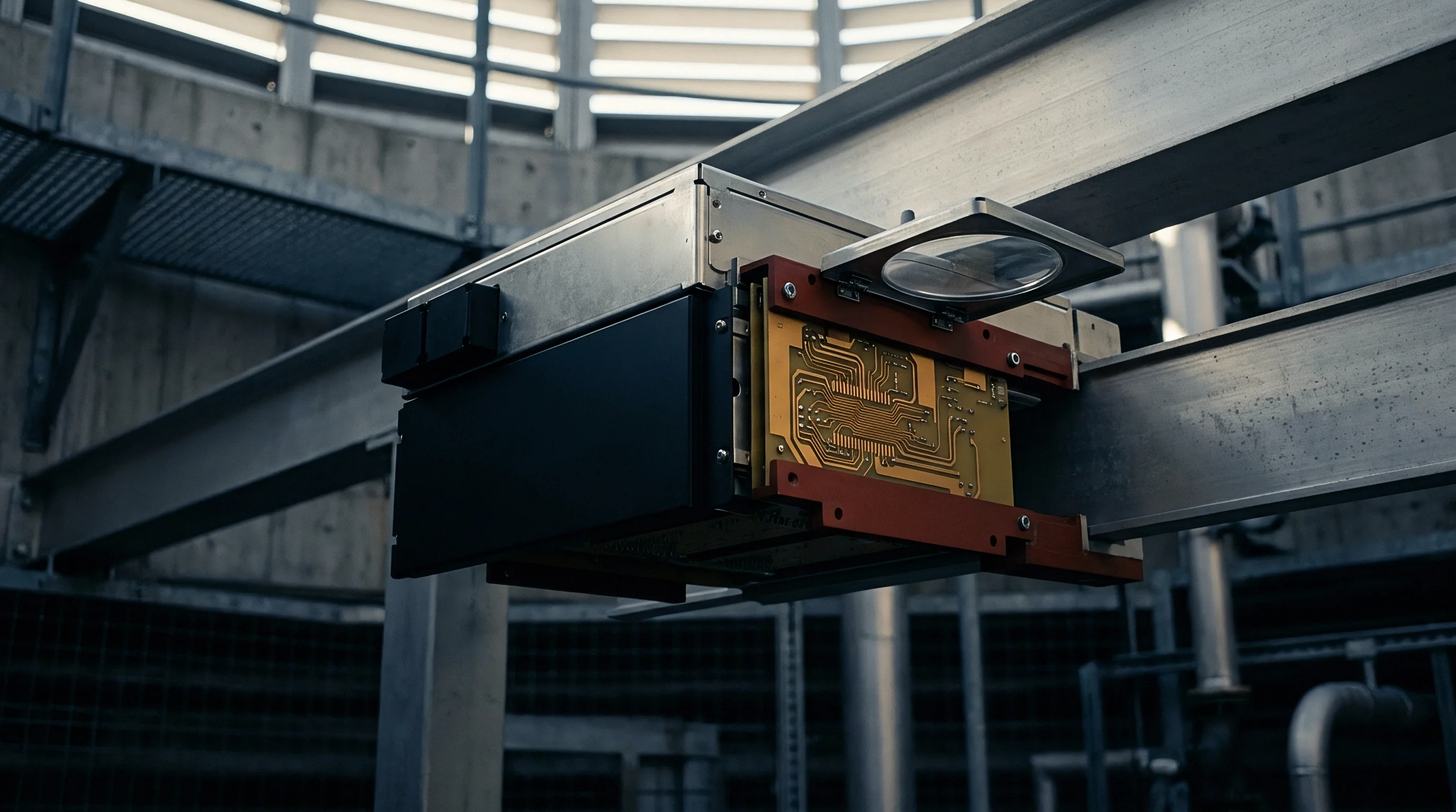
Organic Carriers and Passive Element Placement
Substrates made of high-density glass-reinforced epoxy or ceramic co-fired structures form the physical base for internal component layouts. Adding passive components alters how legal classification rules apply. Decoupling capacitors situated within millimeters of logic dies suppress voltage spikes during high-frequency switching.
Internal component counts directly influence tariff treatment. Inductors created using thin-film copper coils on the die surface itself keep monolithic IC classification. By contrast, separate surface-mount inductors soldered onto the interposer introduce structural elements that customs authorities evaluate against tariff thresholds, directly altering applicable duty rates.
Internal decoupling arrays designed solely to support primary chip functions do not automatically reclassify an encapsulated package as a circuit board assembly.

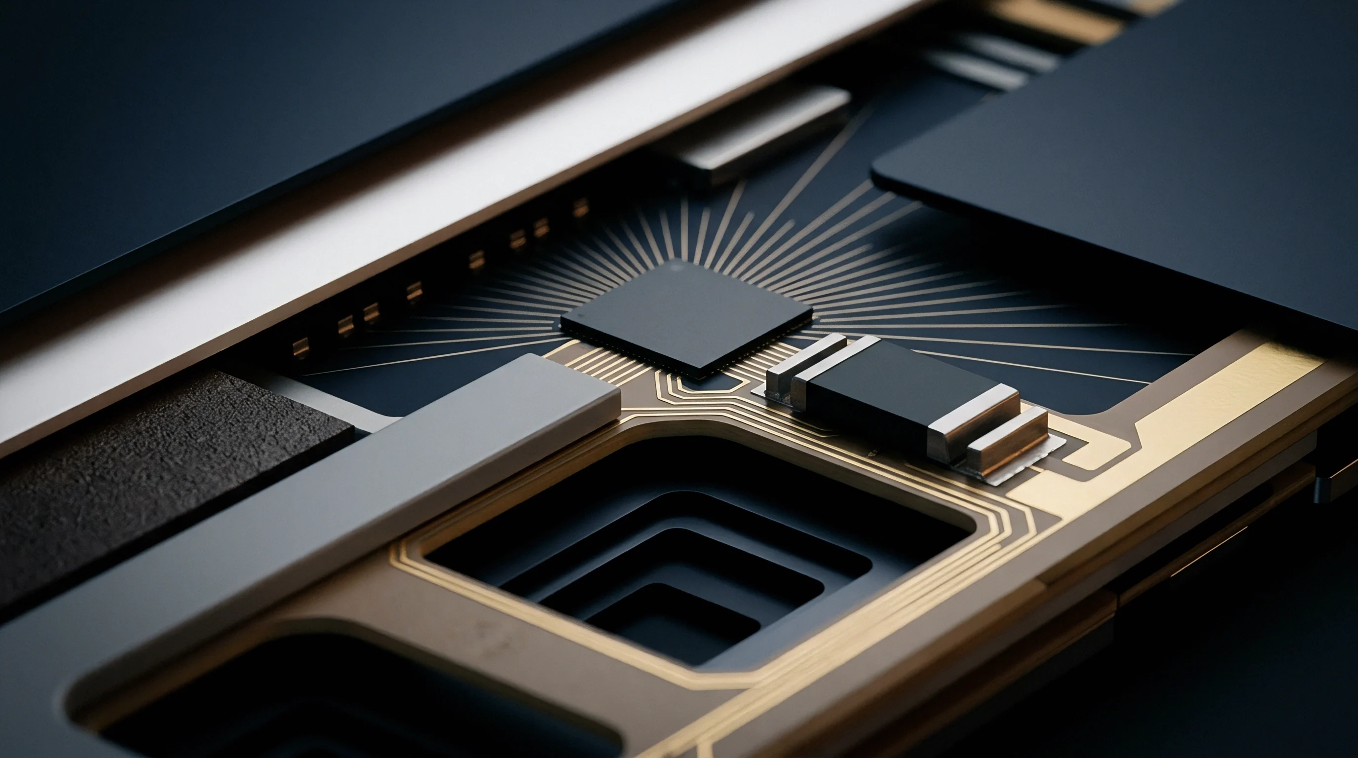
Criteria
Tariff classification relies on explicit statutory thresholds in international schedules. Harmonized System Note 9(b) to Chapter 85 outlines five structural constraints for multi-component integrated circuits, requiring a package to satisfy every condition during physical examination.
| Structural Configuration | HS Code Subheading | ITA Duty Eligibility | Permissible Internal Elements | Disqualifying Features |
|---|---|---|---|---|
| Monolithic Integrated Circuit | 8542.31 / 8542.39 | Duty-Free (0%) | Single semiconductor die, integrated passives on die | Discrete surface-mount resistors, external substrates |
| Multi-Component IC (MCO) | 8542.31 / 8542.39 | Duty-Free (0%) | Multiple IC dies, discrete passives, MEMS devices | Transformers, quartz crystals, battery cells, relays |
| Hybrid Integrated Circuit | 8542.90 / 8548.00 | Variable (0% – 3.5%) | Thick/thin film circuits on ceramic substrate | Unencapsulated PCB substrates, bulky discrete components |
| Electronic Microassembly | 8543.90 / 8548.90 | Standard Rate (2.5% – 6.0%) | Printed circuit boards, relays, crystals, discrete modules | Exceeding Note 9(b) elemental scope boundaries |

Chapter Note Nine Statutory Boundaries
Statutory definitions require multi-component integrated circuits to combine one or more ICs with discrete electronic components. Active silicon dies must carry out the primary electronic function of the package. Substrate layers incorporate buried metallization, while discrete passives like chip resistors, ceramic capacitors, and surface-mount inductors are permitted only if they directly support primary chip functions.
A package containing passive components fabricated on a high-resistivity silicon substrate qualifies under Note 9(b) provided total passive element count does not exceed the integrated semiconductor die count by more than five to one.
Chapter rules exclude specific component types regardless of how small they are or how they mount. Incorporating mechanical switches, quartz crystal resonators, transformers, or standalone battery cells immediately removes a package from Chapter 8542. Adding any prohibited element pushes classification into general electronic microassemblies or host machine subheadings that carry higher baseline duty rates.
Distinguishing Hybrid Circuits from Integrated Multi Component Packages
Manufacturing workflows mark the boundary between hybrid microcircuits and multi-component packages under tariff guidelines. Hybrids use thin- or thick-film technology to deposit passive networks on insulating bases before chips are attached. Multi-component ICs instead pair discrete surface-mount components with silicon dies on leadframes or circuit substrates, fully encased in a molded housing.
Customs auditors inspect internal assembly features to check for misclassification. The following configurations create compliance risks under international trade rules:
- Unencapsulated Module Housing exposes internal circuit elements, ruling out classification under single-package semiconductor tariff lines.
- Prohibited Component Integration adds quartz crystal oscillators or magnetic core transformers to the internal bill of materials.
- Secondary Board Attachment links two pre-packaged components instead of mounting bare silicon dies directly onto a shared substrate.
- Function Breakdown Failure leaves individual ICs working independently without interconnects supporting a unified processing purpose.
Any device containing non-semiconductor magnetic cores or quartz timing elements falls outside Chapter 8542 into host assembly headings, no matter how small the package footprint.

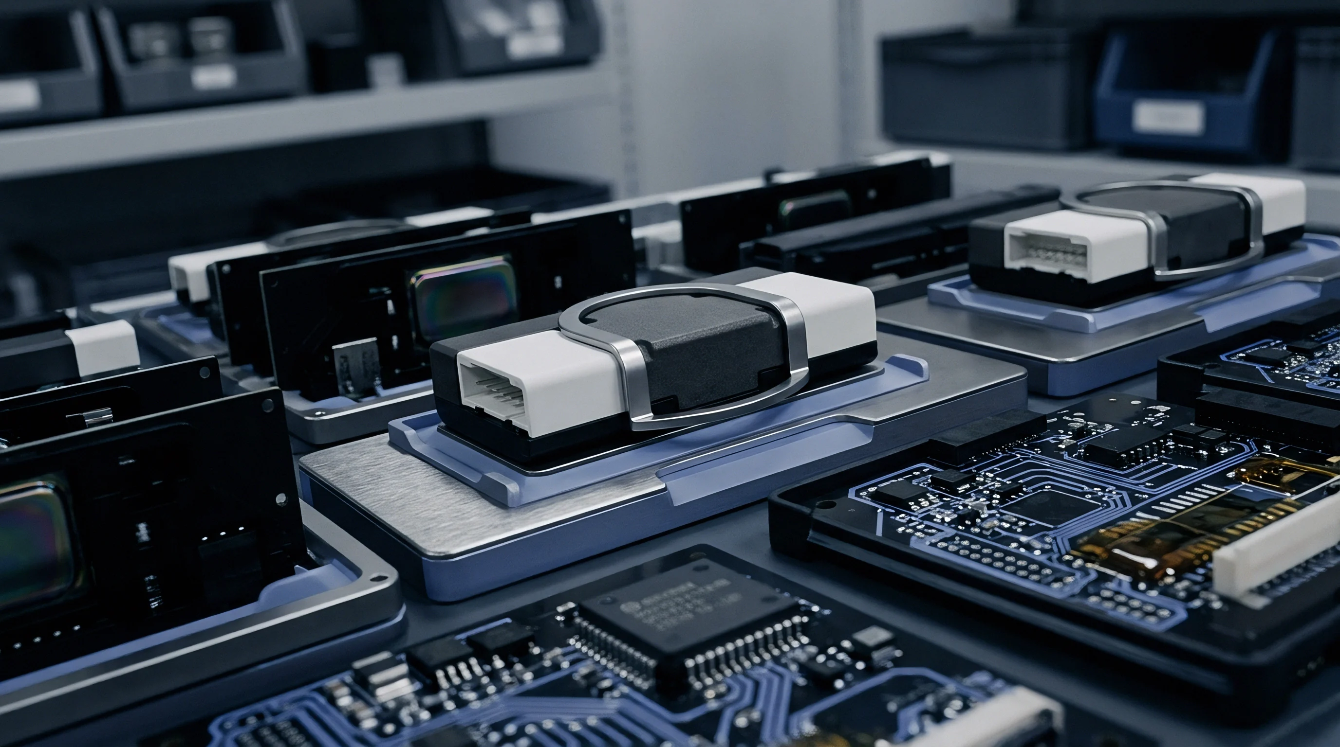
Teardown
Customs laboratories test physical compliance using non-destructive imaging and destructive analysis. Import filings claiming zero-duty status under Information Technology Agreement schedules trigger mandatory sampling whenever documentation lacks sufficient detail on internal structure. Inspection officers redirect suspect shipments to accredited metrology facilities for forensic cross-sectioning.

Destructive Cross Sectioning and Scanning Acoustic Microscopy
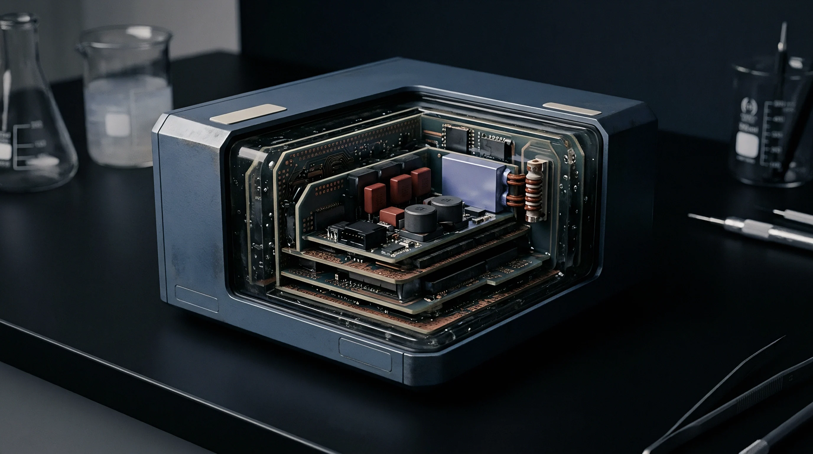
Technicians use C-mode scanning acoustic microscopy to map internal interfaces without opening the plastic casing. Density variations among the mold compound, silicon dies, and discrete capacitors create ultrasonic reflection patterns that reveal internal component counts. X-ray micro-computed tomography builds three-dimensional views of bond wires, substrate traces, and embedded passive elements.
Acoustic imaging revealing unencapsulated ceramic substrates inside an epoxy shell invalidates single-package multi-component integrated circuit declarations.
Physical cross-sectioning verifies layer counts and substrate materials when non-destructive scans prove inconclusive. Precision diamond saws slice through package midsections, exposing internal features for scanning electron microscopy. Microscopic examination confirms whether passive elements are discrete chips or thin-film structures deposited directly on the primary silicon die.

How Are Discrete Component Limits Assessed by Customs?
Documentation must demonstrate that embedded passives merely support the main processing dies rather than forming independent electronic subsystems. Customs laboratories follow a fixed protocol when analyzing submitted micro-component samples:
- Mount the target IC package in epoxy resin matrix and cure at room temperature for twelve hours.
- Grind the cured block along the primary lead alignment axis using silicon carbide abrasive papers.
- Polish the section surface with diamond suspensions down to sub-micron particle sizes.
- Examine substrate interconnects under optical microscopes at magnification levels up to one-thousand times.
- Measure passive element physical dimensions and catalog material composition via energy-dispersive X-ray spectroscopy.
Misclassifying multi-chip packages can trigger shipment seizures, retroactive tariff recalculations, and administrative penalties that quickly inflate landed costs across an entire production run.


Dossier
Maintaining consistent classification across international ports requires a compiled technical binder before commercial shipping begins. Customs brokers present this documentation during entry clearance or post-importation audits to prevent administrative holds at port checkpoints.

Bill of Materials Verification and Process Flow Maps
Technical binders must include an itemized engineering bill of materials listing every component inside the encapsulant. Descriptions clarify whether parts are bare silicon dies, packaged logic chips, or discrete surface-mount passives for customs review.
Manufacturing flowcharts demonstrate that assembly happens in a continuous packaging sequence ending with final encapsulation. Flow diagrams trace raw wafer dicing, die attachment, wire bonding, surface-mount placement, resin transfer molding, and lead trimming. Detailed sequence maps prove compliance with Note 9(b) single-package encapsulation rules.

Binding Tariff Ruling Applications and Evidence Submission
Applying for advance binding rulings eliminates classification ambiguity across destination markets. Customs agencies evaluate these applications against laboratory test reports and technical schematics submitted alongside physical component samples and dimensional drawings.
Ruling submissions require specific technical evidence to pass customs evaluation:
- Uncut Package Samples provide border laboratories with production specimens for acoustic scanning and cross-sectioning.
- Expanded Schematic Diagrams detail internal electrical connections between processing dies and supporting passive networks.
- Cross-Sectional Micrographs supply calibrated visual proof of die placement, interposer layer counts, and wire bond layouts.
- Manufacturer Material Declarations certify mold compound composition, substrate materials, and passive element counts under signature.
Standard procurement contracts require semiconductor suppliers to maintain certified flow diagrams and provide immediate sample access whenever customs audits arise.


Tariff
Proper classification under Chapter 8542 secures zero-duty treatment under the Information Technology Agreement in major trade regions. Assigning packages to general electronic sub-assembly tariff lines instead exposes shipments to base duties from 2.5% to 6.0%, alongside any applicable trade remedy duties, compounding financial exposure on high-volume sourcing programs.
| Declared Heading | Actual Qualifying Status | Base Tariff Duty Rate | Trade Remedy Exposure | Audit Penalty Severity |
|---|---|---|---|---|
| 8542.31.00 | Qualified Multi-Component IC | 0.0% | Exempt | Zero Risk |
| 8542.39.00 | Qualified Multi-Component IC | 0.0% | Exempt | Zero Risk |
| 8543.90.90 | Disqualified Assembly (MCO Fail) | 2.6% | 7.5% – 25.0% | Moderate Duty Recalculation |
| 8548.00.00 | Unclassified Electronic Module | 4.0% – 6.0% | 25.0% | High Penalty + Interest Assessment |
Duty Differential Calculations across Subheading Classifications
Cost modeling illustrates the gap in landed expenses between qualified multi-component ICs and general microassemblies. For instance, importing one million sensor packages priced at five dollars per unit under heading 8542.39 incurs zero base duty, totaling five million dollars in component costs before freight.
Reclassifying that same shipment under subassembly heading 8543.90 at a 2.6% duty rate adds one hundred thirty thousand dollars in base duty liability. Factoring in a 25% trade remedy duty increases total customs payments by one million three hundred eighty thousand dollars on that single product run.
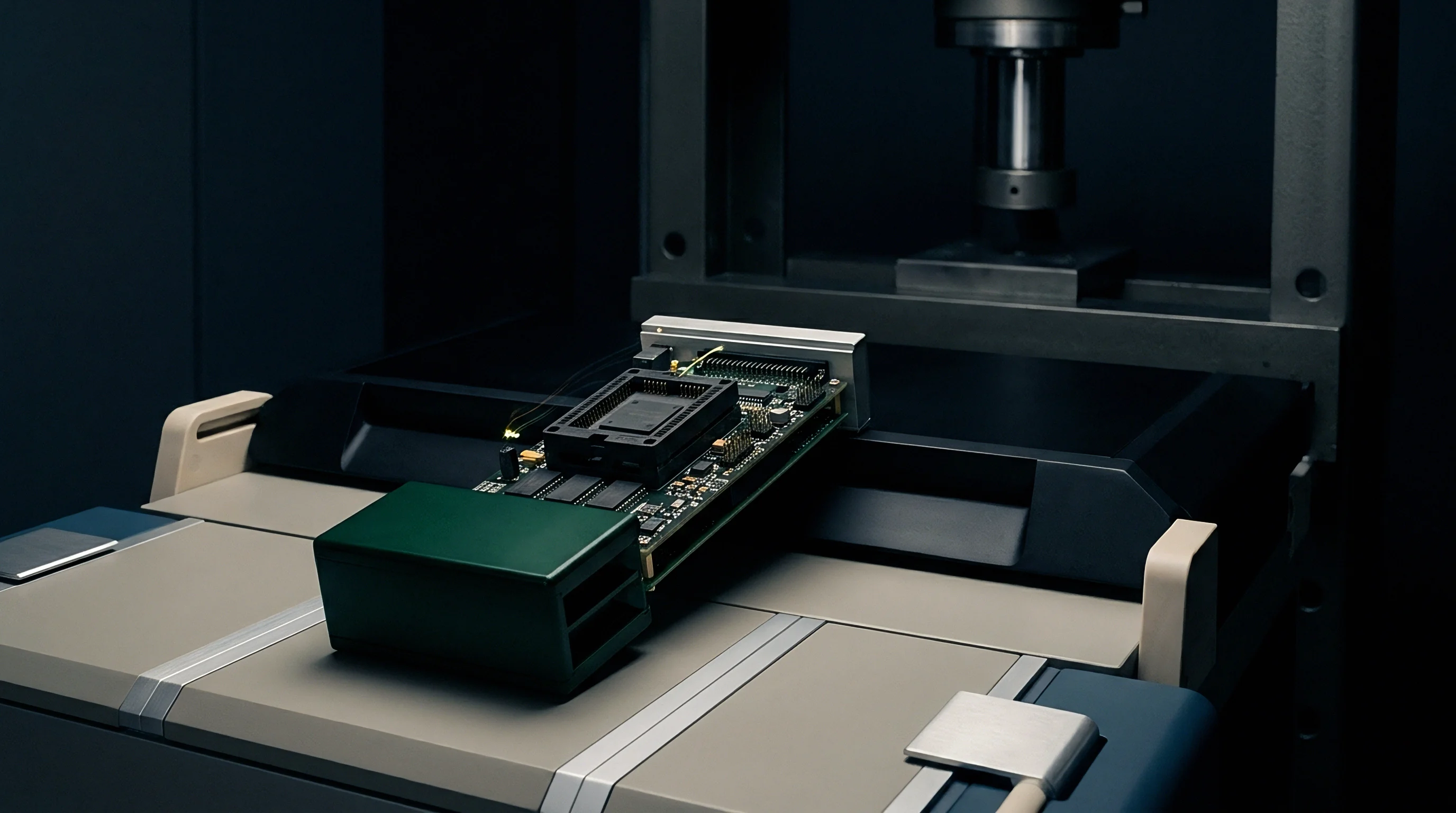
Retroactive Assessment Exposure and Supply Chain Audits
Customs authorities review entry declarations retroactively across three- to five-year lookback windows. Audit teams demand physical teardown records, bills of materials, and ruling documentation for all imported semiconductor packages, applying penalties to any misclassified entries.
Failing to substantiate Chapter 8542 eligibility triggers retroactive assessments across all historical entries within the audit window. Authorities calculate compound interest on unpaid duties and can assess administrative penalties up to two hundred percent of the total duty shortfall. Importers under audit must verify every internal package component against Chapter Note rules or face complete reclassification.
What specific test data or structural proof will customs authorities demand when micro-inductors integrated onto organic substrates cross international borders under revised Harmonized System revisions?