Meaning
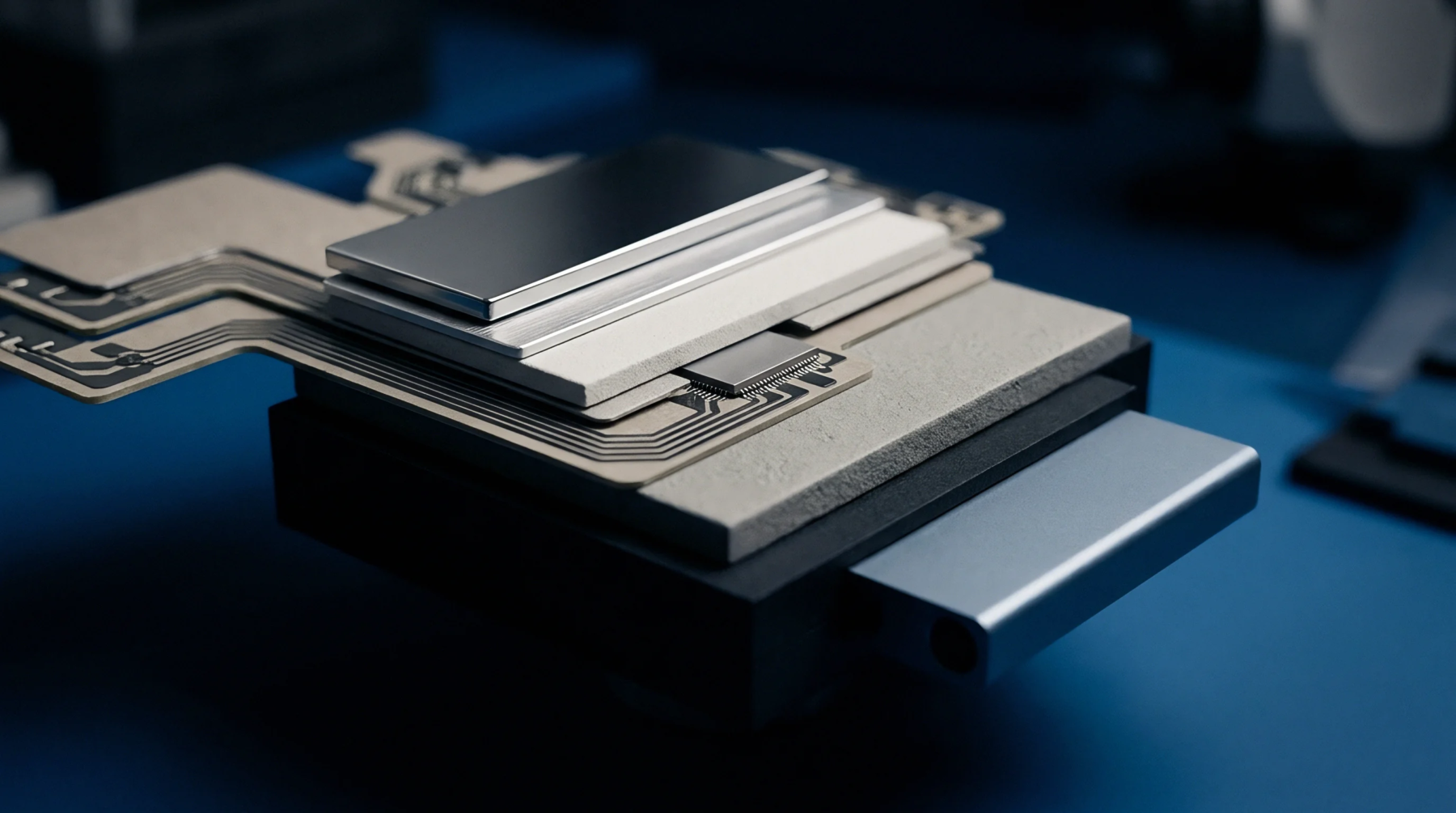
Semiconductor assembly relies on an interconnect method where an unpackaged integrated circuit is inverted and mounted directly onto a substrate using conductive bumps. Through bare die flip chip bonding, the silicon rests face down, which minimizes path lengths and parasitic inductance. This setup provides superior high frequency electrical performance and supports high density inputs.
Interconnect Geometry
Substrate design must align with the fine bump pitch of the silicon, often requiring sub fifty micrometre trace spacing. During assembly, the bare die flip chip bonding process relies on precise robotic placement to align the bump array with the substrate terminals before thermal or ultrasonic energy completes the connection. The resulting reduction in package footprint prevents inductive loop issues.
Heat Dissipation
Thermal management is facilitated by the exposed backside of the silicon, allowing direct contact with a heat sink or thermal interface material. Because the active circuitry sits closer to the substrate, heat can also escape through the copper bumps into the circuit board itself.
Joint Reinforcement
Liquid epoxy is dispensed after the interconnect is formed to fill the remaining void between the chip and substrate. This underfill material protects the electrical joints from moisture and distributes mechanical stress caused by different rates of thermal expansion.