Bare Metal Register State Isolation for Undocumented Microcontroller Silicon Errata
Hardware-enforced register state isolation mitigates undocumented microcontroller errata by enforcing atomic memory barriers and shadow state verification.


Trap
New silicon steppings often carry undocumented register anomalies that only surface in narrow corner cases. Silicon errata happen when physical gating diverges from the bus specification, leaving memory-mapped I/O blocks holding unpredictable logic states. Bare-metal firmware is especially vulnerable: control lines, interrupt flags, and configuration registers flip without warning.
Standard compiler sanity checks miss the problem entirely, because the core executes structurally valid memory instructions while the underlying hardware delivers corrupt bit patterns.
Internal bus matrix bridges route memory transactions between core execution units and peripheral controllers. During clock transitions down to low-power modes, internal synchronization latches can drop volatile register bits. A read-modify-write sequence aimed at a timer control block might silently clear an adjacent status bit packed into the same memory word, while propagation delays across internal buses trigger setup and hold violations on flip-flops across operating ranges from minus forty to eighty-five degrees Celsius.
Many unlisted silicon anomalies stem from asynchronous clock domain crossings deep on the die, where a peripheral on a low-speed crystal writes into a status register on the high-speed system bus. The resulting metastability can lock intermediate logic levels across physical latches and freeze hardware timers without an explicit bus fault.

Silicon Hardware Defects in Memory Mapped Registers
Microarchitectural faults change register behavior without triggering CPU faults. An ARM Cortex-M or RISC-V core will step through its instruction pipeline normally while peripheral hardware drifts away from the state software expects. In safety-critical loops, that divergence causes peripherals to miss deadlines or produce erratic outputs without ever tripping a hard fault.
Under heavy electrical noise or rapid supply voltage swings, unmapped register instabilities become far more pronounced. During transient brownouts, flash controller state machines can latch corrupt wait-state values into configuration registers, stalling execution and causing cold resets to fail before an interrupt vector can fire.

Asynchronous Bus Clock Crossings and Shadow Latches
Peripheral bridges connect separate frequency domains through intermediate shadow latches. When software asserts an enable bit, the underlying gating has to settle before the core issues its next memory transaction. Without register isolation, back-to-back writes collide with the shadow latch during an active transfer window.
- Shadow latch bit flip Clock synchronization failures cause transient bit inversions in peripheral configuration registers while shifting frequencies.
- Read modify write collision Concurrent core writes and peripheral status updates drop interrupt clears across shared register words.
- Power gating register leak Power gating drops peripheral register contents without restoring baseline configuration vectors when waking from sleep.
- Interrupt vector context bleed Exception flags hold active logic states across context switches, trapping core handlers in persistent loops.
When fault interrupts fire late, silicon errata sheets typically classify the underlying behavior as outside normal operating bounds, leaving external software to absorb the timing delays manually.


Vault
Hardware-enforced state containment shields volatile memory-mapped registers from bus-level glitches. Building this isolation vault means wrapping bare-metal drivers in deterministic atomic boundaries, memory protection unit rules, and dedicated static shadow RAM buffers. To isolate the physical register, driver code must block direct core access to raw peripheral addresses while configuration is underway.
Routing configuration accesses through an abstraction layer bound to protected memory allows software to verify integrity before committing state to silicon. After each write, the wrapper reads back the physical address, checks it against a golden register image stored in secure static memory, and executes an explicit memory barrier before handing execution back to the application.

Atomic Memory Access and Peripheral Bit Gating
Bit-banding aliases and dedicated bit-set/bit-clear registers prevent read-modify-write races. Updating individual control bits through standard read-modify-write sequences risks corruption whenever peripheral hardware updates adjacent status flags mid-instruction.
Without atomic access, context switches trigger faults during bitwise updates. Enforcing atomic writes ensures that single-bit configuration shifts execute in one cycle without touching neighboring fields. Where hardware lacks native bit-band aliasing, peripheral registers require global interrupt locks or atomic load-store assembly primitives to maintain isolation.
Hardening registers against silicon errata demands hardware-enforced memory isolation rather than software convention alone.

Memory Protection Unit Region Isolation Mechanics
Memory protection units divide the address map into distinct privilege tiers. Applying MPU rules over peripheral regions prevents unprivileged application code from firing off raw register writes that trigger known silicon bugs.
| Isolation Level | Latency Penalty | Silicon Overhead | Errata Mitigation Coverage | Hardware Dependency |
|---|---|---|---|---|
| Software Shadow Mirror | 12 to 18 Clock Cycles | 1.2 KB Static RAM | Register Corruption Detection | None Plain C Code |
| Atomic Bit-Banding Alias | 2 to 4 Clock Cycles | 0 KB Static RAM | Read-Modify-Write Collision Prevention | Hardware Bit-Band Controller |
| MPU Privilege Barrier | 24 to 36 Clock Cycles | 512 Bytes Flash Memory | Unauthorized Peripheral Memory Access | Hardware MPU Core Unit |
| Hardware DMA Ring Vault | 45 to 60 Clock Cycles | 2.0 KB Static RAM | Asynchronous Bus Crossing Drift | Multi-Channel DMA Engine |
Peripheral register boundaries hold firm when application code touches only shadow registers in system memory. A dedicated kernel task then manages synchronization between shadow RAM and physical address space, validating state before flushing values out to the bus.
Direct, unverified register access breaks down whenever silicon errata drop pending flags or corrupt bits during bus transactions.


Shield
Defensive firmware wrappers use assembly barriers to keep register drift from spilling into global state. Low-level routines rely on data memory barriers, data synchronization barriers, and instruction synchronization barriers to lock down execution order around peripheral accesses. This assembly boundary prevents pipeline hazards where aggressive compiler reordering might expose intermediate register transitions.
Defensive wrappers rely on naked assembly primitives that scrub working core registers around interrupt entry and exit to prevent memory lockups. On entry, volatile registers must be purged of leftover peripheral state before stale data can leak into thread stack frames.

Assembly Wrapper Layer for State Isolation
Optimizing compilers often coalesce register reads or discard back-to-back loads assuming hardware registers behave like normal static memory. Silicon errata break that model completely, since peripheral state shifts on the die without the compiler’s knowledge.
A thirty-two bit state verification check adds six clock cycles of overhead per peripheral context switch at eighty megahertz.
Assembly-level shields prevent compiler over-optimization by qualifying register pointers as volatile and wrapping every transaction in explicit memory barriers. When DMA channels stream peripheral payloads directly into static RAM, software must invalidate cache lines and issue flush barriers to preserve data integrity across unshielded internal buses.

Context Switch Register Scrubbing Sequence
Context switches open prime windows for register corruption. The following sequence runs on every context transition to keep peripheral state stable.
- Disable global interrupts through context status registers before crossing into isolated driver space.
- Read back peripheral configuration registers to force an immediate bus flush.
- Execute a data memory barrier instruction to guarantee completion of all pending register writes.
- Compare register contents against the golden mirror stored in secure static RAM.
- Re-enable global interrupts once the register checksum validates.
Even if static RAM maintains parity, skipping register verification during rapid context switches leads to silent corruption across application memory, eventually triggering spontaneous brownouts or unrecoverable core lockups.
Probe
Validating register isolation under realistic electrical stress calls for automated test benches that can trigger bus collisions and transient supply dips. Probing debug access ports over Serial Wire Debug or JTAG lets external hardware monitor memory-mapped registers in real time without stalling the processor core. Uncovering undocumented silicon bugs means coupling power-rail glitch injection with continuous read-back loops across both bare and isolated drivers.
Verification harnesses run continuous boundary scans to catch register drift as operating conditions fluctuate. By comparing physical register values against verified shadow RAM over millions of cycles, test engineers uncover silicon errata well before boards reach production lines.

Automated SWD Register Sampling Jigs
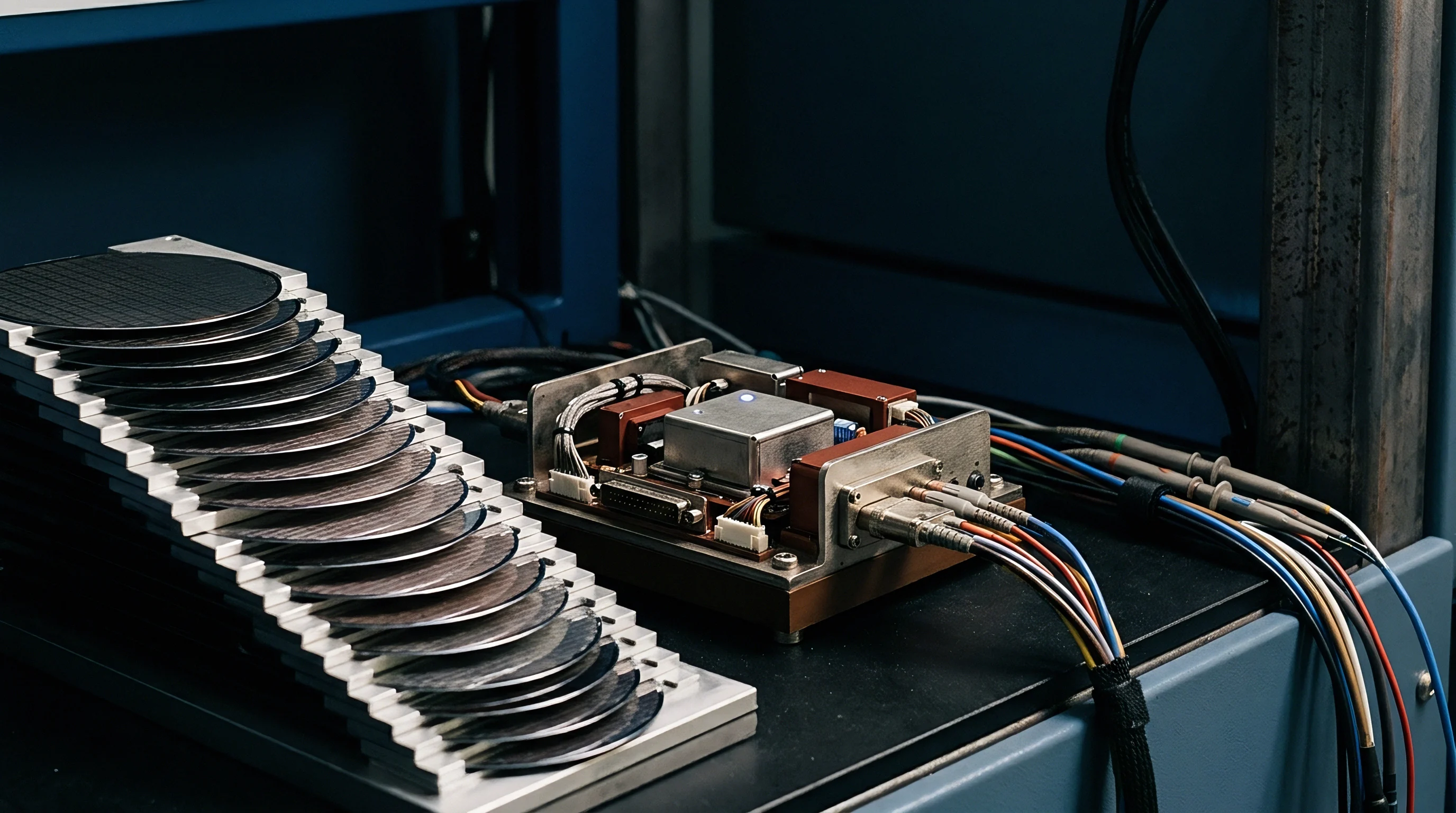
Automated hardware-in-the-loop fixtures tie debug probes directly into build servers. The jig cycles core voltages, generates high-speed peripheral traffic, and tracks debug access port registers to catch unmapped bit shifts as they occur.
How Does Hardware Register Scrubbing Prevent Undocumented Transients?
Register scrubbing periodically refreshes memory-mapped registers from validated golden patterns stored in protected static RAM. Running as high-priority tasks, scrubbing routines overwrite physical registers at set intervals, wiping out volatile bit shifts from latch instabilities before the peripheral drifts out of specification.
| Test Profile | Injection Mechanism | Target Peripheral | Sample Duration | Observed Failure Mode |
|---|---|---|---|---|
| Voltage Rail Ripple | 100 mV 10 MHz Injection | UART Control Block | 10 Million Cycles | Baud Rate Generator Drift |
| Clock Domain Glitch | Phase Shift 45 Degrees | SPI Configuration Unit | 50 Million Cycles | Clock Polarity Flip |
| DMA Bus Contention | Multi-Channel Saturation | Advanced Timer Block | 100 Million Cycles | PWM Duty Cycle Distortion |
| Power Gated Wakeup | 1 kHz Deep Sleep Cycles | Real Time Clock Register | 5 Million Cycles | Prescaler Register Reset |
Design transfer documentation must spell out the exact register verification criteria used to certify module stability before committing capital to production tooling.
- Assembly source registers map Complete address map of all peripheral registers covered by isolation wrappers and bit-band aliases.
- JTAG verification test scripts Test bench scripts for injecting clock glitches and sampling memory-mapped registers.
- Errata trigger timing specifications Precise bus timing parameters that reliably provoke register corruption.
- Static memory checksum tables Pre-calculated checksum tables used by scrubbing routines to validate shadow mirrors.
Which automated testing methodology definitively proves that a specific undocumented silicon erratum has been fully isolated across all operational thermal ranges?


Covenant
Sourcing contracts for custom modules and white-label boards need explicit boundaries around silicon errata remediation. Buyers entering turnkey or semi-custom manufacturing deals take on substantial financial exposure when vendor board support packages fail to isolate undocumented register defects. A comprehensive transfer package defines non-recurring engineering line items, IP boundaries, and clear deliverables for custom isolation wrappers.
Clause twelve of the standard integration agreement assigns firmware patching expenses to the module buyer once silicon engineering samples receive formal signoff.
Because module firmware must absorb physical errata, supply contracts must keep unit component pricing separate from engineering deliverables. When microcontrollers arrive with unlisted die defects, determining who pays for low-level isolation development comes down entirely to how the statement of work defined the initial scope.

Silicon Errata Risk Allocation and NRE Scope
Non-recurring engineering quotes must detail the deliverables needed to isolate undocumented silicon faults. Turnkey manufacturing agreements routinely omit driver hardening, leaving buyers on the hook for custom engineering when production units encounter register instability in the field.
Semi-custom manufacturing models offer a practical compromise by sharing engineering liability between the module vendor and the buyer. Under this setup, the vendor delivers hardened bare-metal abstraction drivers as a contracted milestone, while the buyer maintains full ownership of application source repositories.

Transfer Packages and Firmware Maintenance SLAs
Design transfer packages must bundle all low-level source files, reproducible build toolchains, automated hardware-in-the-loop test scripts, and raw bill of materials data. Any package that omits assembly register wrappers locks the buyer to a single supplier, blocking second-source manufacturing if component availability tightens.
| Scope Level | NRE Price Range | Firmware Deliverables | Errata SLA Coverage | IP Ownership Scope |
|---|---|---|---|---|
| Turnkey Reference | $5,000 to $12,000 | Pre-Compiled Binary Blobs | Vendor Standard Errata Only | Factory Retains All IP |
| Semi-Custom Hardened | $25,000 to $45,000 | C Source Drivers and Headers | 36 Months Custom Patching | Shared Licensing Right |
| Full Design Transfer | $60,000 to $110,000 | Full Assembly Source and Jigs | Lifetime Firmware Escrow | Buyer Owns All Source IP |
| Estimates based on typical thirty-two bit ARM microcontroller custom module engineering scope contracts as of 2024. | ||||
Standard supply agreements warrant hardware conformity only against published vendor datasheets, effectively carving out unlisted silicon errata unless explicit register isolation testing requirements are written into the technical specification annex.