Silicon Stepping Qualification Basics for Wireless Subsystem Integrators
Silicon stepping qualification requires register-level ID verification, driver patch synchronization, RF harmonic re-testing, and contractually defined NRE cost allocation.

Wafer
Semiconductor foundries update silicon through mask revisions, categorized as base or metal steppings. A base-level stepping change ~ such as moving from release A0 to B0 ~ replaces optical masks across active diffusion layers and interconnect tracks. This alters transistor gate dimensions, substrate doping profiles, and internal parasitic capacitances inside RF synthesis circuits.
A metal-level stepping revision, like A0 to A1, changes only upper copper or aluminum routing layers while leaving underlying transistor geometries intact. Integrators encounter these steppings when vendors fix hardware bugs, update internal ROM bootloaders, or tune analog power amplifiers for better yield. Which type of stepping occurred dictates whether the host platform needs a simple register-level update or a full RF recalibration over temperature.
Host microcontrollers read silicon revisions during boot by querying identification registers over PCIe, SDIO, or SPI. Design teams hard-code these revision values into read-only register addresses that expose major stepping codes, metal tweaks, and ROM tags. When a wireless System-in-Package or IC powers up, driver firmware parses those bits to branch its initialization, load phase-locked loop tuning tables, or push patch binaries into internal RAM.
Misidentifying the stepping results in wrong driver settings, which can leave RF transceivers running with mismatched registers or unstable bias currents.
| Revision Type | Mask Layers Changed | Silicon Register ID Example | Host Firmware Impact | RF Performance Shift |
|---|---|---|---|---|
| Base Stepping Change (A0 to B0) | Diffusion, Poly-Silicon, and Metal (100%) | 0x0020 to 0x0100 | Major driver branch update, memory map changes, patch rebuild | Output power drift +/- 1.5 dB, phase noise shifts up to 3 dBc/Hz |
| Metal Stepping Change (A0 to A1) | Top Interconnect Layers Only (10-20%) | 0x0020 to 0x0021 | Minor table patch, fixed ROM address overrides | Negligible RF shift, minor power consumption reduction (< 3%) |
| ROM Code Revision (Base Fixed) | Metal Mask for Metal-ROM or Fuse Array | 0x0020 (ROM version flag 0x02) | Driver patch routine removal, updated boot loader hooks | Zero RF shift, altered timing on host handshakes |
Base steppings often address power distribution issues or memory leaks in embedded ARM or RISC-V cores. Re-synthesizing the clock tree to fix those issues shifts the digital noise spectrum radiated into nearby low-noise amplifiers on the die. Moving a module to a B0 stepping can therefore cause small sensitivity drops at specific carrier frequencies where digital switching harmonics relocated.
Catching these shifts takes register-level verification and baseline spectrum checks before releasing updated modules to high-volume production.
Ignoring base silicon changes during integration leads to high field-failure rates once host software writes outdated initialization tables to altered physical registers.


Errata
Hardware fixes delivered through stepping revisions alter host driver dependencies and existing register workarounds. Silicon vendors list known chip flaws and patch recommendations in errata sheets. When a new stepping arrives, workarounds built into older host drivers can become redundant or actively harmful.
For example, a write sequence that settled a phase-locked loop on A0 might trigger clock instability or synthesizer lock failure on B0, where the internal lock timer was redesigned in hardware.
Host Driver Dependencies and Patch Firmware
Host software built on Modular Driver Architectures (MDA) executes stepping-dependent binary blobs at boot. The driver reads the hardware stepping register, selects the right patch binary, and loads it into the wireless chip’s RAM before releasing the core from reset. If the driver lacks support for the new stepping, it either falls back to legacy code or aborts initialization altogether.
This requires keeping host drivers, OS kernel updates, and incoming module inventory strictly in sync.
Unchecked firmware patches loaded onto the wrong silicon revision disrupt internal calibration and cause intermittent packet drops.

RF Synthesizer Shifts and Tuning Parameters
Analog stepping updates often adjust passives, op-amps, or bias trees in the radio front-end. These circuit changes modify power amplifier transconductance and LN-amp impedance, requiring re-validation of calibration parameters stored in non-volatile memory or driver code. Transmit power target tables, EVM compensation coefficients, and receiver gain stage boundaries can all shift between revisions.
- Transmit Power Table Drift causes RF power output to breach regulatory limits or drop below link budget thresholds at band edges.
- Receiver Gain Disparity skews RSSI reporting, causing host connection managers to trigger premature cell handoffs.
- Low-Power Sleep Current Spikes occur when updated power management state machines fail to enter deep sleep without updated register triggers.
- Clock Synthesizer Phase Noise Degradation occurs when legacy loop-filter settings run on modified voltage-controlled oscillators.
- OTP Calibration Byte Mismatch corrupts factory calibration data reads when register offset maps shift between major steppings.
Skipping audits of driver patch binaries against incoming physical steppings leads to unstable wireless links and high current draw in battery-powered deployments.
Metal-level stepping changes are often documented as fully backward compatible even when register workarounds that legacy host drivers still depend on during boot sequences are removed.

Margin
Transmitter radiation profiles shift when foundries tweak process parameters or re-spin masks for yield. Changes to output-stage bias networks alter harmonics, intermodulation products, and out-of-band emissions. Regulatory bodies such as the FCC and ETSI set strict limits on RF emission drift, so integrators using modular certifications must determine whether a stepping change qualifies as a Class I Permissive Change or requires Class II re-testing at an accredited lab.
Spurious Emissions and Modular Certification Thresholds
A small increase in clock harmonic amplitude can push emissions past regulatory limits and invalidate modular approvals. Integrators measure conducted and radiated emissions across all supported channels in anechoic chambers. If peak spurious emissions on the new stepping rise more than 3 dB above the original filing, regulations require a formal re-submission with complete test data.
Modular certification rules allow permissive changes without full recertification as long as output power stays within 0.5 dB of the original filing.
| RF Performance Parameter | Measured Delta Boundary | Regulatory Filing Category | Required Integration Testing |
|---|---|---|---|
| Peak Conducted Output Power | Within +/- 0.5 dB | Class I Permissive Change | In-house verification, baseline lab log retention |
| Peak Conducted Output Power | Exceeds + 0.5 dB | Class II Permissive Change | Accredited lab testing, formal FCC/ISED filing update |
| Radiated Spurious Harmonics | Increase < 3.0 dB (below limit) | Class I Permissive Change | Engineering test report update, internal risk audit |
| Radiated Spurious Harmonics | Increase >= 3.0 dB or limit breach | Full Re-Certification Required | Complete radio re-testing across all operational modes |

Thermal Dissipation and Current Draw Variances
Process tweaks that shrink die area can increase current density and thermal resistance at active gates. A B0 stepping running at peak transmit duty cycles might run 5 °C hotter than A0 under identical conditions. Integrators need thermal imaging and current profiling to verify junction temperatures stay within spec.
Higher temperatures also degrade frequency stability, causing crystal oscillator load capacitance to drift during long transmit bursts.
- Mount the wireless module with the new silicon stepping onto a calibrated thermal evaluation board inside a temperature chamber.
- Connect an automated power analyzer to measure sleep current, receive current, and peak transmit current at maximum duty cycle.
- Run a continuous ten-minute transmit burst at full power while sweeping chamber temperature from -40 to +85 °C.
- Record spurious emissions, carrier frequency drift, and EVM performance at 10 °C increments.
- Compare the spectral data against baseline measurements to confirm compliance with worst-case margins.
If silicon changes push power levels past certified limits, commercial contracts generally shift lab re-qualification fees, filing costs, and line downtime penalties back to the module vendor.

Pipeline
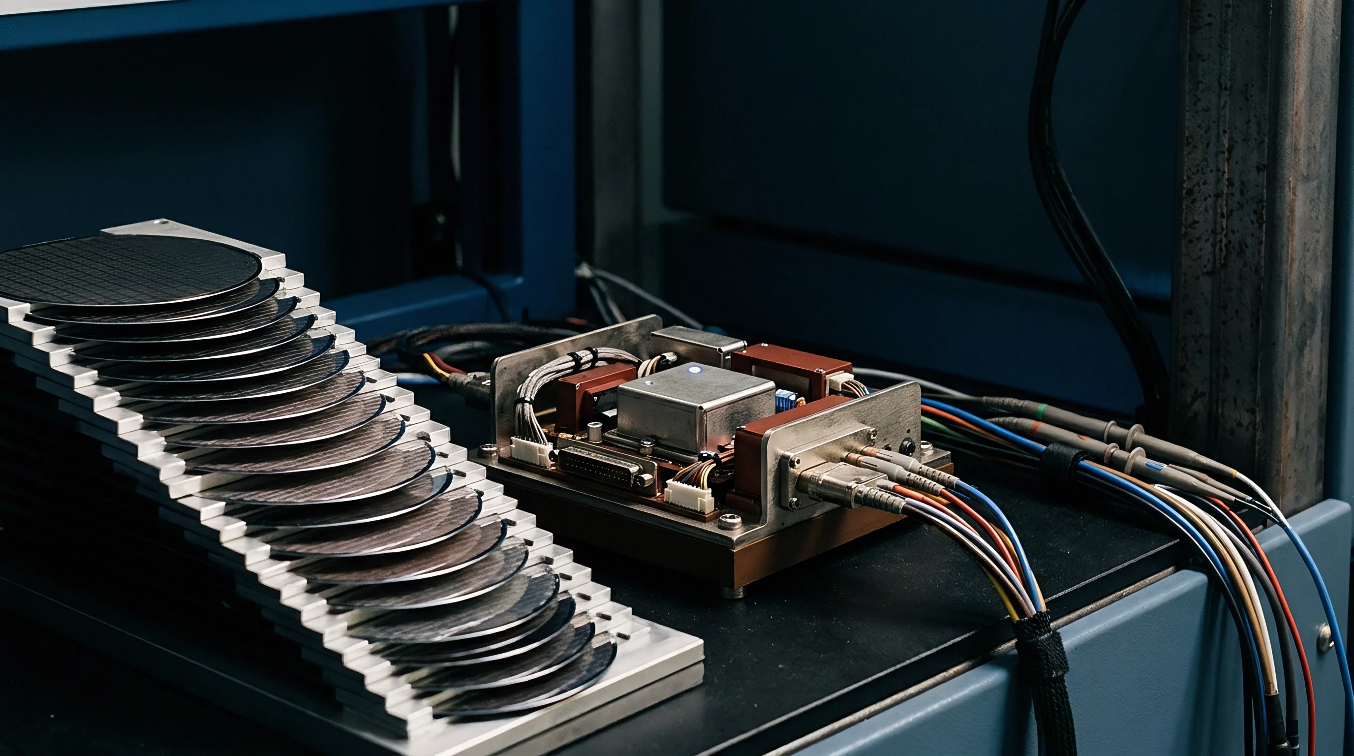
Assembly lines rely on validation protocols to confirm that new silicon revisions integrate without interrupting automated flashing or test routines. Product Change Notifications (PCNs) give advance notice of stepping transitions, listing last-time-buy dates, transition windows, and sample availability. Engineering teams need parallel testing pipelines to validate sample lots before volume shipments arrive.
Uncoordinated transitions risk factory downtime, mixed inventory, and yield drops.
How Does a Stepping Revision Alter Factory Scripts?
Automated test equipment runs command-line scripts to flash initial firmware, program bootloaders, and write MAC addresses into non-volatile memory. A stepping change can alter target RAM register maps, OTP register offsets, or flash programming voltages. Scripts that hardcode hardware addresses must be updated and verified on pre-production samples.
Running un-updated scripts risks permanently bricking microcontrollers during OTP programming.
Programming routines on new silicon steppings require dual-stage register checks to prevent OTP memory corruption during production flashing.
Product Change Notification Lifecycle and Dual Sourcing
Handling overlap periods when old and new steppings ship concurrently requires tight version tracking. Integrators use serial number encoding and BOM tracking to map which stepping is inside each finished unit. Where dual-sourcing is used, host application software must identify board revisions at runtime and adjust firmware paths without needing separate assembly lines.
- Hardware Revision Identifiers route through physical pull-up resistors so host microcontrollers can detect the stepping immediately.
- Dynamic Firmware Selection embeds multiple patch binaries in host storage to allow runtime driver configuration.
- Incoming Quality Audits run automated register ID checks on sample trays from every incoming semiconductor batch.
- Buffer Stock Management isolates legacy stepping inventory to cover active production during validation.
Procurement teams face immediate timeline friction when software validation turns up unannounced register changes in production samples during PCN windows.


Accounting
Qualifying a silicon stepping incurs non-recurring engineering costs across software development, lab testing, regulatory filings, and line audits. Contracts must establish financial responsibility among buyers, integrators, and vendors before work starts. Turnkey sourcing agreements usually assign re-qualification costs to the module manufacturer, while custom contracts pass those expenses to the buyer.
Calculating the full cost of a transition requires accounting for engineering hours, external lab fees, and scrapped materials.

Non Recurring Engineering Breakdown for Requalification
A qualification effort requires effort across RF design, firmware development, and quality assurance. Re-testing an updated stepping involves firmware patches, thermal testing, script updates, and regulatory filings. The table below shows representative engineering hours, external facility fees, and expense ranges for qualifying a wireless subsystem stepping.
| Qualification Phase | Primary Engineering Task | Resource Commitment (Hours) | External Costs (USD) | Financial Risk Owner |
|---|---|---|---|---|
| Driver Refactoring | Patch integration, register map updates, regression testing | 80 to 160 hours | $0 (In-house) | Integrator / Buyer |
| RF Lab Validation | EVM, sensitivity, harmonic distortion, thermal sweeps | 40 to 80 hours | $2,000 (Chamber rental) | Integrator / Buyer |
| Regulatory Filings | Accredited lab testing, C2PC documentation, agency submission | 20 to 40 hours | $8,000 to $18,000 | Module Vendor / Buyer |
| Factory Pilot Run | Test script updates, OTP flashing audit, 500-unit pilot batch | 30 to 60 hours | $3,000 (Scrap & downtime) | Factory / Integrator |
Warranty Liability Allocation and Obsolescence Amortization
Field failures from unannounced stepping changes create clear liability exposure. Supply contracts need to specify whether a vendor-initiated stepping change counts as a material alteration. If a vendor ships a new stepping without written authorization and causes instability or non-compliance, contract terms typically require vendor coverage for recalls, scrap, and remediation.
Managing obsolescence on older inventory requires defining clear consumption windows during PCN discussions.
Engineering teams allocate dedicated NRE budgets for regulatory permissive change testing before approving volume production cutovers.
Integration risk scales with the extent of custom driver modifications and proprietary calibration code embedded in host software.