Meaning
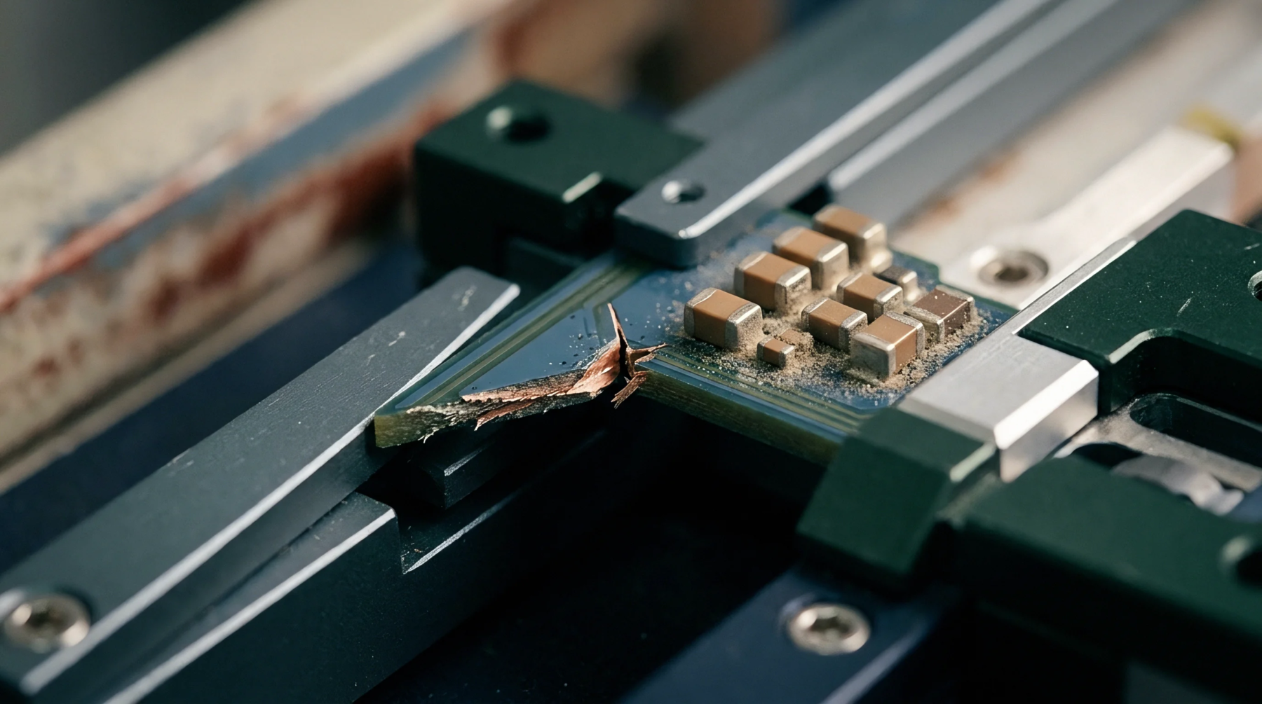
Physical deformation of microelectronic connections occurs during the high-pressure injection of plastic molding compound into a semiconductor package. This phenomenon, known as bond wire sweep, bends the fine gold or copper wires that connect the silicon die to the leadframe. It creates a risk of internal electrical short circuits when adjacent wires make contact.
Packaging engineers test for this movement using three-dimensional X-ray imaging after the molding process is complete.
Mechanical Displacement
Viscous forces from the flowing epoxy molding compound exert a drag on the suspended wires, pushing them in the direction of the flow front. Bond wire sweep depends on the velocity of the liquid compound and the viscosity of the formulation. Long wire loops are particularly vulnerable to this force because the flow generates a greater moment arm at the anchor points.
Minimizing the loop length or increasing the wire diameter helps to reduce the displacement, which maintains the required physical separation inside the package.
Plastic Encapsulation
Injection parameters must be carefully regulated during the transfer molding step to prevent excessive wire deflection. Lower transfer speeds reduce the drag forces but might cause the mold to cure before the cavity is filled. Finding the correct parameter balance is essential for yield.
Production Failure
Electrical failure results when the displaced wires touch each other or break at the neck of the ball bump. This leads to immediate opens or latent reliability hazards that arise during thermal cycling. Component qualifications require strict adherence to maximum sweep percentages.