Meaning
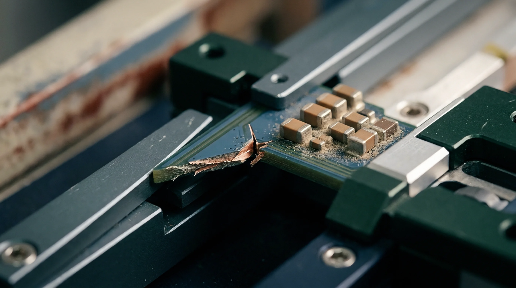
Separation between substrate layers, copper foils, or encapsulation materials in printed circuit board assemblies marks a structural failure mode that degrades mechanical integrity and electrical continuity. Moisture absorption and thermal stress during surface mount reflow soldering frequently induce delamination along weak material interfaces. The boundary of this physical defect includes inter layer separation within laminate stacks and package encapsulation lift, but excludes surface solder joint fractures.
Thermal Stress
Rapid vapor expansion from entrapped moisture creates localized internal pressure inside multi layer circuit boards during high temperature soldering cycles. If this vapor pressure exceeds the adhesion strength of epoxy bonding resin, delamination separates adjacent fiberglass plies or copper trace layers. The resulting air gaps disrupt dielectric constants, alter microstrip impedance, and introduce intermittent open circuits under mechanical vibration.
Environmental stress screening subjects completed modules to thermal shock testing to force latent structural separations to appear before field deployment.
Quality Control
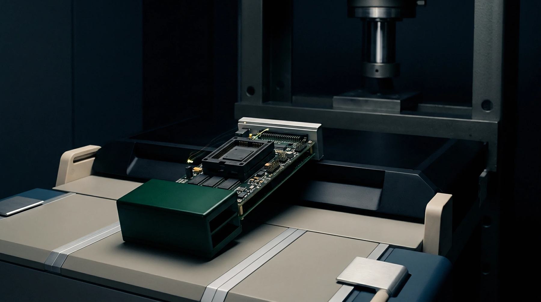
Acoustic micro imaging and cross sectional metallography evaluate board lamination quality during supplier lot acceptance. Ultrasonic inspection detects subtle acoustic impedance variations across interface layers, pinpointing voids caused by delamination without destroying the module. Quality assurance engineers document these acoustic scans in the incoming inspection report to reject sub standard substrate batches before component population.
Reliability Risk
Unintended separation of substrate layers creates pathways for conductive anodic filament growth across adjacent high voltage traces. Moisture ingress into internal voids causes catastrophic dielectric breakdown during humidity bias testing.