Meaning
High-purity silicon dioxide in non-crystalline form acts as a low-loss dielectric substrate for high-frequency microelectronic circuits. Millimetre-wave and sub-terahertz packaging designs use fused silica to minimize signal attenuation and maintain phase consistency across long transmission lines.
Material Property
Amorphous molecular structure gives this glass a very low coefficient of thermal expansion and high optical clarity. The dielectric constant of fused silica remains stable across a wide temperature range, which prevents resonant frequency shifts in patch antennas. Low tangent loss ensures that electromagnetic energy is not converted into unwanted heat within the packaging.
Integration Performance
System designers choose this substrate for applications that demand high thermal stability and structural rigidity. Surface acoustic wave filters built on fused silica can operate at extreme power levels without experiencing the substrate breakdown common in organic laminates.
Manufacturing Challenge
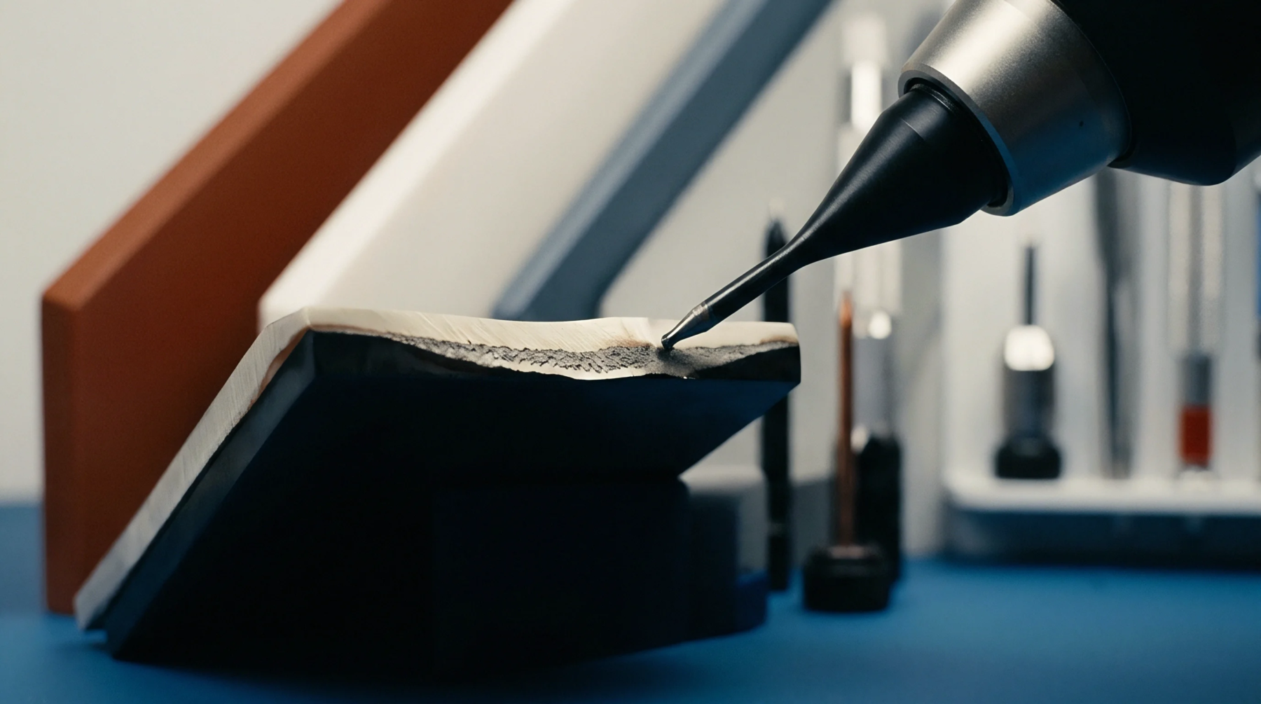
The mechanical hardness of this material makes traditional mechanical drilling and dicing processes expensive and prone to micro-cracking. Advanced manufacturing processes utilize laser ablation or chemical etching to create precise via holes and smooth circuit trenches in fused silica layers. These fine-line geometries are essential for fabricating microstrip lines that meet the impedance tolerances of sub-terahertz systems.
Achieving high-yield assembly requires specialized metallization techniques to ensure that copper layers adhere securely to the smooth glass surface without peeling during thermal cycling.