Meaning
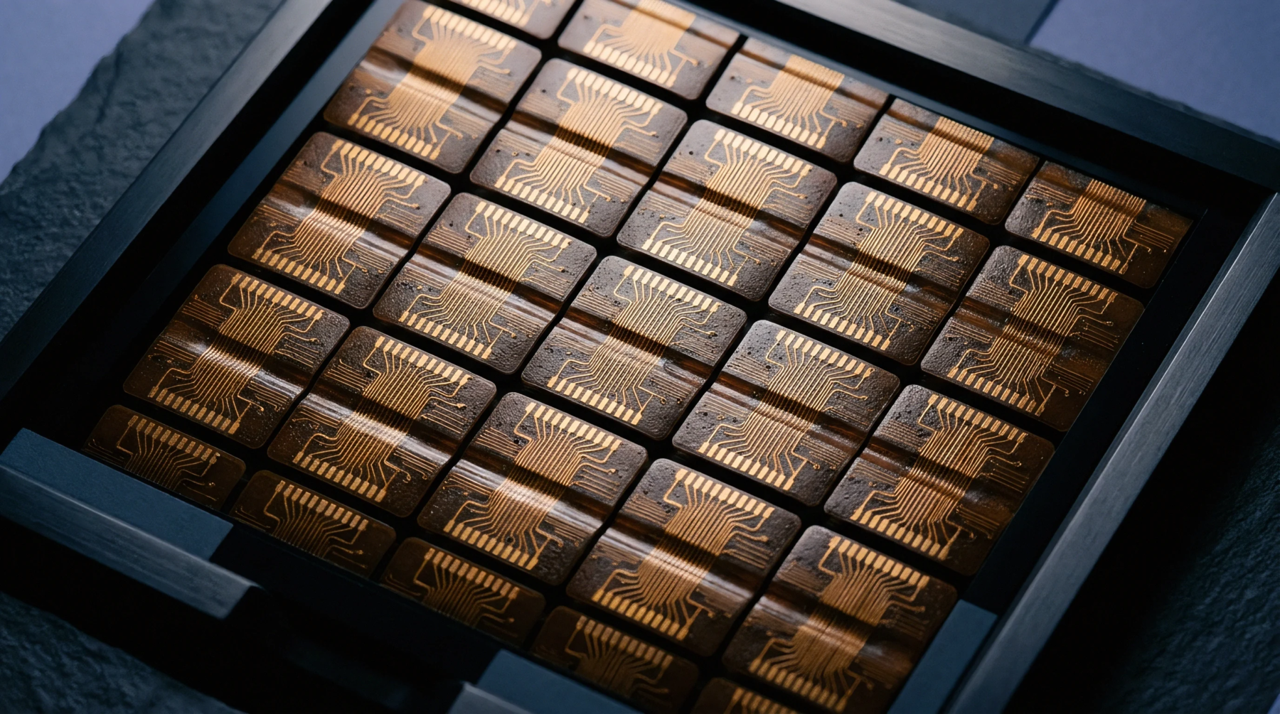
Metal structures provide the electrical connections and structural support for a semiconductor die inside its plastic housing. Most high volume connectivity modules utilize leadframe packaging to route signals from the silicon chip to the printed circuit board. This technology consists of a central pad for the die and a series of leads that extend outward to the pins of the device.
It is utilized primarily for low to medium pin count components where cost and thermal performance are the main considerations.
Thermal Management
Thermal dissipation is a primary benefit of using a copper alloy frame as the base of the component. Heat generated during radio transmission travels through the leadframe packaging to the external solder joints and into the motherboard. This path prevents the silicon from overheating and maintains the stability of the wireless signal.
Mechanical Support
Manufacturing steps involve die attachment and wire bonding followed by the transfer of a resin over the entire assembly. The leadframe packaging process requires precise alignment of the gold or copper wires that connect the chip to the metal leads. After the resin hardens, the individual parts are cut from the larger metal strip and the leads are bent into the final shape.
Assembly Reliability
Using leadframe packaging ensures that the electrical path remains intact during the life of the smart device.