Meaning
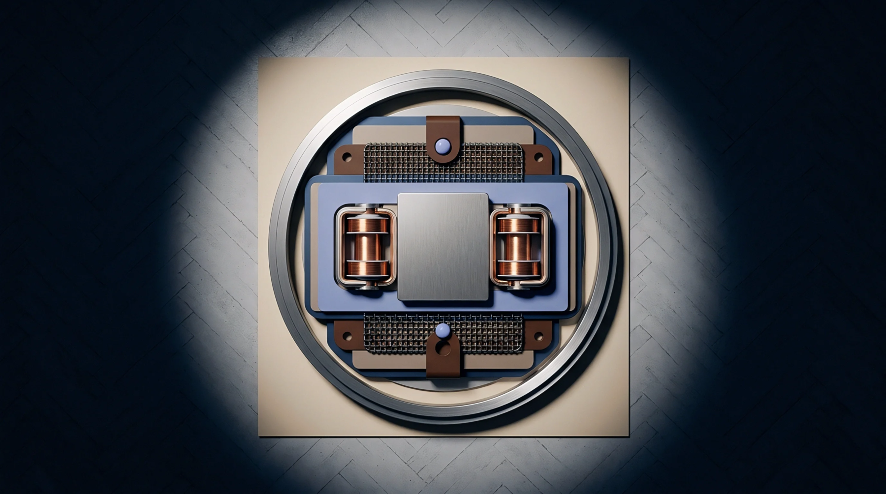
A specialized manufacturing process involves the integration of bare silicon dies, passive components, and sub-substrates into a single compact housing or system-in-package. Doing micro-electronic module assembly requires cleanroom environments and high-precision pick-and-place systems to handle sub-millimeter components. It bridges the gap between semiconductor fabrication and standard printed circuit board assembly.
Process Stage
The workflow begins with substrate preparation and adhesive dispensing, followed by wire bonding or flip-chip soldering. Each stage of the micro-electronic module assembly is monitored by automated optical inspection.
Precision Requirement
Placing microscopic dies demands sub-micron alignment accuracy to avoid bridging the tiny bond pads. Even a tiny misalignment can cause short circuits or open connections that ruin the entire module. Modern flip-chip mounters use advanced vision systems to align the solder bumps with the substrate pads before thermal reflow.
Thermal Management
Packaging multiple heat-generating silicon dies into a tiny footprint requires excellent thermal transfer designs. During assembly, high-conductivity thermal interface materials are applied between the dies and the metal shield. This path prevents local hotspots that would otherwise degrade performance or shorten the operating life of the device.
Consequently, thermal qualification of these packages is a major step in the overall design approval process.