Meaning
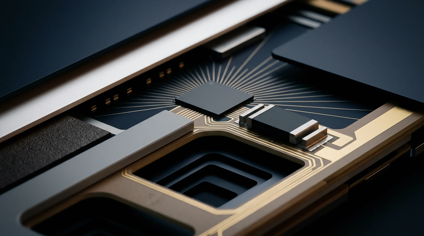
The high-density encapsulation of sub-millimetre silicon dies and passive devices is engineered to minimize the footprint of electronic sub-assemblies on a printed circuit board. Implementing microcomponent packaging enables the integration of advanced radio-frequency front-ends and multi-sensor modules into wearable devices where physical volume is constrained.
Mechanical Structure
This structural design protects the delicate internal circuitry from humidity and mechanical shock while providing electrical interconnects. The technology behind microcomponent packaging utilizes wafer-level chip-scale designs or fan-out configurations to eliminate the need for traditional plastic or ceramic leadframes. It allows for a smaller interconnect distance, which enhances high-frequency signal integrity.
Thermal Control
Managing heat dissipation within such confined physical boundaries represents a major engineering challenge for developers. When power-dense transceivers use microcomponent packaging, the localized thermal energy must be dissipated through ground vias to prevent localized overheating. This requires the integration of high-conductivity thermal interface materials between the package and the module shield.
Production Integration
Specialised pick-and-place equipment is required to assemble these tiny modules with high positional accuracy during factory assembly. The tiny solder balls of microcomponent packaging are highly sensitive to solder paste deposition thickness, demanding high precision during the stencil printing phase. Process verification through automated optical inspection is necessary to ensure that the microscopic interconnects do not suffer from bridging or open circuits.