Meaning
Poly-para-xylylene polymers deposited via vapor deposition polymerization provide thin, pinhole-free conformal barriers across electronic board assemblies. Parylene c incorporates a single chlorine atom on its aromatic benzene ring, balancing electrical insulation with low permeability to moisture and corrosive atmospheric gases. The application boundary covers fully populated circuit assemblies, wire bonds, and microelectromechanical systems prior to enclosure assembly.
It stops short of separable contact surfaces, optical sensors, and acoustic ports, which demand physical masking before deposition begins.
Deposition Dynamics
Vacuum chambers vaporize solid dimer precursor material at elevated temperatures before cracking the gas into reactive monomers within a high-temperature pyrolysis furnace. Gaseous monomer enters the ambient-temperature vacuum chamber, polymerizing spontaneously upon all exposed surfaces without solvent carriers or thermal curing stresses. A uniform coating thickness forms over sharp conductor edges, underneath low-standoff surface mount components, and within blind vias.
Liquid conformals retract from sharp corners due to surface tension, whereas vapor phase deposition avoids meniscus effects entirely.
Dielectric Isolation
Excellent electrical properties make the polymer an effective barrier against high-voltage breakdown in space-constrained designs. Parylene c features a high dielectric strength exceeding five thousand volts per mil and maintains a stable dielectric constant across radio frequencies. The pinhole-free film prevents dendrite formation and electrolytic corrosion between tightly spaced traces subjected to salt fog, sulfur gas, and high humidity.
Low dielectric dissipation factors minimize insertion loss when traces carrying high-frequency radio signals receive conformal protection.
Masking Validation
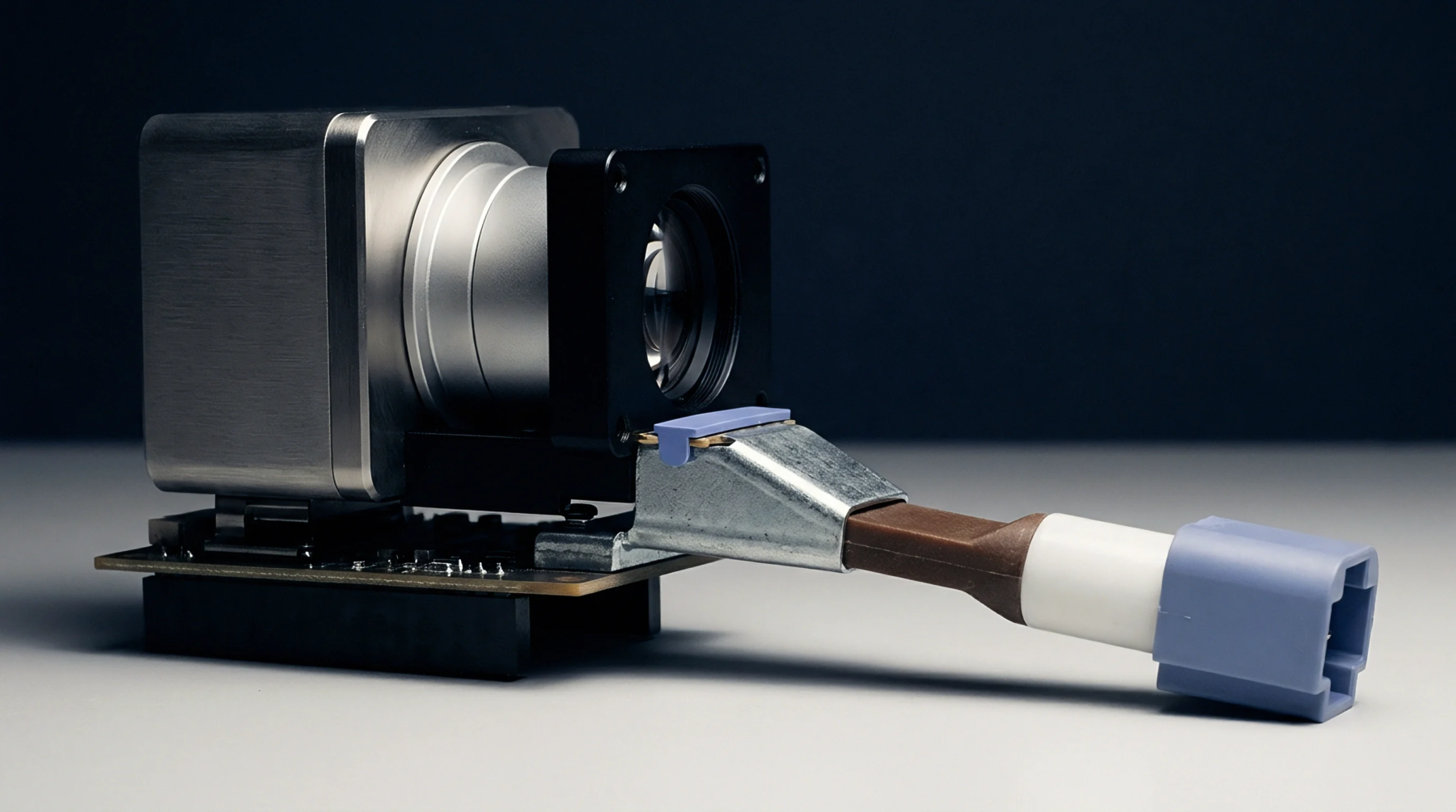
Masking integrity requires stringent pre-process preparation using specialized adhesive tapes, elastomeric boots, or photocurable peelable masks. The vaporous monomer penetrates openings smaller than one micron, meaning improper sealing allows unwanted coating over connector contacts and ground pads. Thickness verification takes place on sacrificial silicon witness coupons placed alongside product boards, measured via spectroscopic ellipsometry or contact profilometry.
Quality release requires tape adhesion pull tests and cross-sectional inspections to confirm uniform deposition across shadowed components.