Meaning
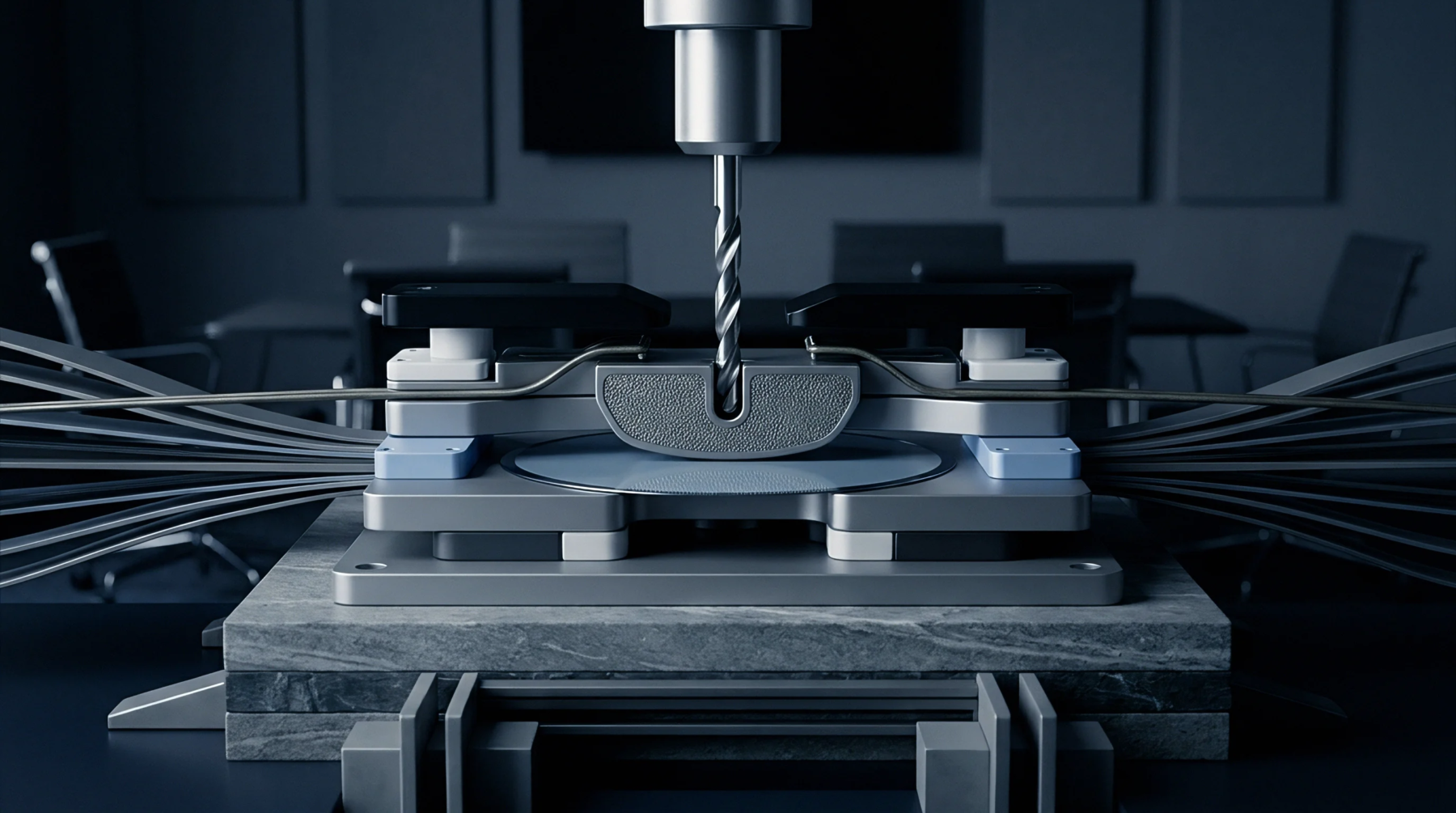
A specialized glass plate containing the magnified master image of a circuit pattern is used in photolithography to manufacture semiconductor devices. The reticle acts as a high-precision stencil that defines where light passes through to expose the photoresist on the silicon wafer. It holds the layout of a single chip or a small group of chips, which is projected and demagnified by the stepper machine.
This component is essential for defining the microscopic structures on the silicon.
Lithographic Transfer
High-intensity ultraviolet light passes through the clear regions of the glass to replicate the design onto the substrate. Each reticle is aligned with extreme precision to ensure that subsequent layers match the previously printed patterns. This alignment is critical for the correct assembly of multi-layer microchips.
Mechanical Handling
Robotic arms transfer the glass plate from storage pods to the exposure chamber to prevent human contamination. The reticle must be kept in a clean environment and protected by a thin protective pellicle. This shielding prevents airborne dust particles from settling on the pattern.
Defect Impact
Dust particles on the glass surface can cause a repeating pattern defect across the entire wafer. If the reticle has a defect, every single field exposed through it will contain the same physical error. This reduces the yield of functional chips and increases manufacturing costs.