Sourcing Ready Modules versus Custom Discrete Circuit Design
Sourcing ready modules minimizes upfront NRE and regulatory risk for mid-volume hardware, while custom discrete designs optimize unit landed cost at scale.

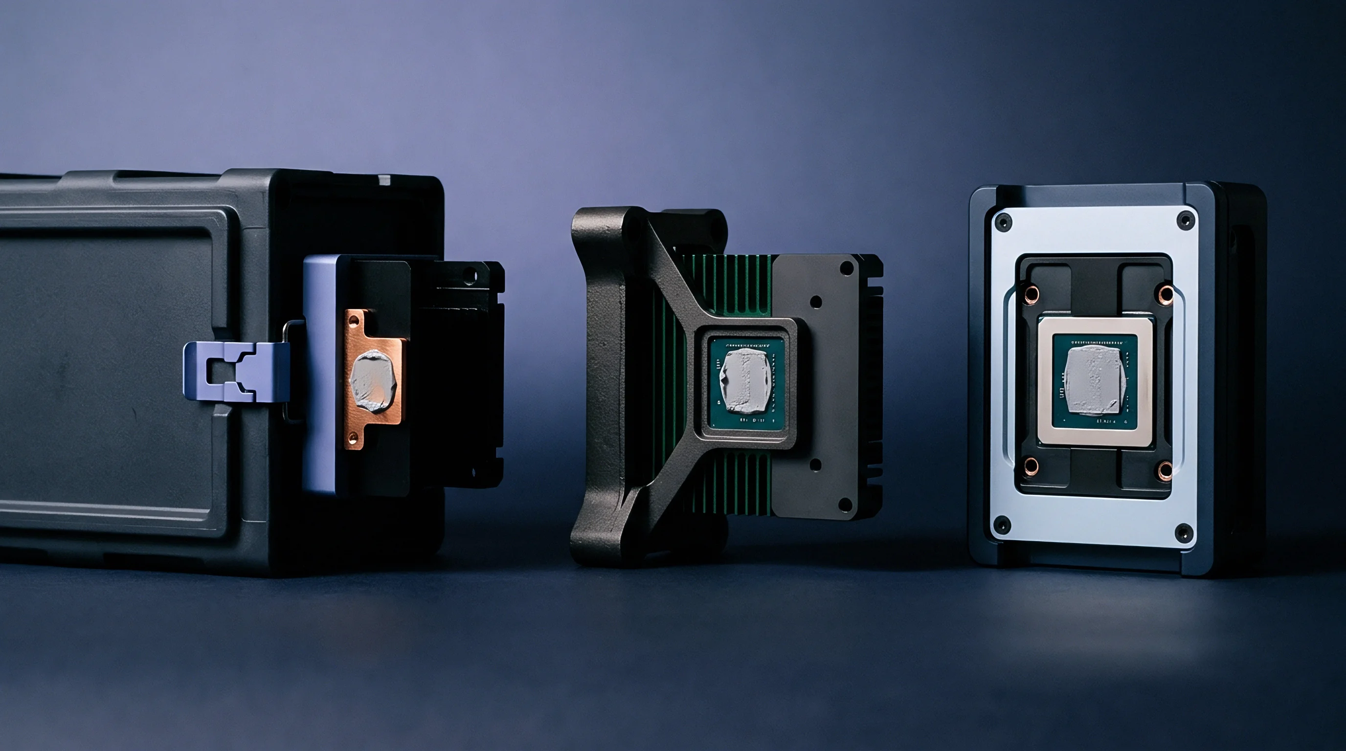
Silicon
Choosing between an off-the-shelf wireless module and a discrete circuit layout sets the physical and financial path for a hardware product. Surface-mount modules in shielded LGA or castellated packages push high-frequency RF complexity off the host board. A discrete layout puts the transceiver, crystal resonator, passive matching network, and power management ICs straight onto the main system board.
That architectural choice dictates whether engineering effort focuses on basic board interconnects or component-level RF tuning.
Integrated radio modules pack the die, matching components, bandpass filters, and reference clocks into a single substrate. Vendors tune internal traces to present a clean fifty-ohm interface at the pins. With a discrete layout, every RF node is exposed to PCB manufacturing tolerances, dielectric shifts, and stray copper coupling.
A slight trace variation between the transceiver output and chip antenna can alter return loss, degrade harmonic suppression, and drop receiver sensitivity.
Coplanar waveguides with ground planes are the standard layout structure for routing RF across host PCBs. Hitting a target impedance requires tight control over substrate thickness, trace width, copper weight, and spacing to neighboring ground pours. Standard four-layer FR-4 boards can see dielectric constant variations up to ten percent between manufacturing batches.
Those shifts pull a nominal fifty-ohm trace down to forty-four ohms or up to fifty-seven, generating standing wave reflections at the antenna port.
In discrete RF designs, decoupling capacitor placement dictates power network performance. Switching transceivers draw sharp current bursts during transmission. Placing decoupling capacitors more than two millimeters from power pins adds enough trace inductance to sag local supply voltage during bursts.
Those voltage dips introduce phase jitter into local oscillators, degrading modulation accuracy and risking compliance failures on error vector magnitude. Modules avoid this exposure by burying high-frequency ceramic caps fractions of a millimeter from the die inside the shielded cavity.
Shielding can mask underlying grounding flaws during initial testing.
Thermal management takes very different routes in packaged modules versus discrete layouts. High-power amplifiers generate concentrated heat that must bleed into the PCB stackup. Modules pull heat away through central ground pad arrays on their underside into the main board’s ground planes.
Discrete designs give engineers room to space out power amplifiers, LNAs, and power management ICs, using thermal via fields and heavier two-ounce copper to pull down junction-to-ambient thermal resistance.
| Parameter | Turnkey Ready Module | Semi-Custom Reference Layout | Discrete Circuit Design |
|---|---|---|---|
| Primary Substrate Footprint | 15 mm x 22 mm fixed package | 12 mm x 15 mm layout block | 8 mm x 10 mm component cluster |
| Board Layer Requirement | Standard 2-layer or 4-layer FR-4 | Controlled 4-layer FR-4 stackup | Controlled 4-layer or 6-layer HDI |
| Impedance Matching Risk | Internalized to module assembly | Shared via layout geometry | Fully borne by host PCB layout |
| Non-Recurring Engineering (NRE) | $5,000 to $15,000 | $25,000 to $60,000 | $80,000 to $200,000 |
| Development Time to Prototype | 4 to 8 weeks | 12 to 16 weeks | 24 to 36 weeks |
| Unit Bill of Materials Cost | $3.50 to $7.00 per unit | $2.20 to $4.50 per unit | $1.10 to $2.30 per unit |

Impedance Matching and Passive Element Selection
High-frequency radio designs require precise impedance matching between the transceiver output and the radiating element. Discrete implementations rely on Pi- or T-networks built from low-ESR inductors and ceramic capacitors. Using components with five percent manufacturing tolerances introduces impedance variations across production runs, shifting the resonant frequency band and causing power loss.
Unshielded trace routing passing within three millimeters of the switching inductor creates similar coupling patterns.
Parasitic capacitance between SMT pads and internal ground layers distorts theoretical network calculations. On a standard four-layer board with a 0.2-millimeter outer dielectric, a typical 0402 pad adds roughly 0.2 picofarads of parasitic capacitance to ground. RF engineers must offset pad parasitics by adjusting component values over repeated VNA measurements on prototype hardware.
Off-the-shelf modules eliminate this bench labor by tuning internal matching networks on low-loss ceramic substrates during manufacturing.
Crystal selection introduces another stability risk in discrete radio designs. RF standards mandate carrier frequency accuracy within narrow parts-per-million limits over broad temperature ranges. Discrete layouts need matched load caps, careful isolation of crystal traces from high-speed digital lines, and physical separation from onboard power management.
Stray board capacitance across crystal terminals alters the oscillation frequency, shifting emissions outside assigned spectrum masks and dropping links with base stations.

Printed Circuit Board Stackup Constraints
Substrate layer ordering sets up signal return paths, shielding, and power delivery performance. A discrete wireless design requires at least four board layers to maintain continuous ground reference planes directly below signal traces. Removing ground planes under high-frequency traces forces return currents into long loops, turning power traces into accidental slot antennas that radiate spurious emissions.
Pre-packaged modules permit two-layer host boards in simpler, low-speed products by containing high-frequency return paths within the module substrate.
A four-layer board substrate with a 0.1-millimeter top dielectric layer requires a 0.18-millimeter trace width to achieve a fifty-ohm transmission line impedance.
Trace width control becomes critical when host boards use thin outer dielectrics to reduce package thickness. Board houses enforce trace width tolerances of plus or minus ten percent on standard production runs. On a thin dielectric layer, a ten percent trace width drift shifts characteristic impedance by four ohms, altering RF coupling to the antenna port.
Discrete designs demand controlled-impedance fabrication callouts, raising basic PCB manufacturing costs across all production volumes.
Using microvias for high-density interconnects introduces structural manufacturing complexity. Fine-pitch micro-BGA packages (0.4-millimeter pad pitch) in discrete layouts demand via-in-pad plating and laser drilling. These advanced fabrication processes increase raw PCB costs by thirty to fifty percent over standard through-hole via designs.
Module packages with 1.0-millimeter or 1.27-millimeter pad pitches allow standard mechanical drilling and standard trace rules on host PCBs.
High-frequency RF performance relies heavily on layout rigor.
Layout geometry near the antenna feedline controls overall radiation efficiency. Discrete matching networks require strict ground-plane keep-out zones to prevent unwanted capacitive loading. Running copper pours, battery terminals, or metal enclosures inside specified clearance zones detunes the antenna, causing severe range degradation and excessive battery draw.
Module reference designs specify exact keep-out dimensions, though mechanical enclosure constraints frequently compromise antenna clearance in host board integrations.
- Uncontrolled Ground Plane Discontinuities Split ground planes directly underneath high-speed digital or RF traces force return currents around slot openings, expanding loop area and driving radiated interference.
- Inadequate Thermal Relief on Ground Pads Direct copper connections to large ground pours without thermal spokes sink heat during reflow soldering, causing cold solder joints and intermittent connections.
- Sub-Optimal Crystal Oscillator Layout Long traces between the quartz crystal, load capacitors, and transceiver pins pick up digital switching noise from adjacent buses, inducing phase noise in the RF synthesizer.
- Incorrect Decoupling Capacitor Placement Routing power traces through via structures before reaching decoupling capacitor pads invalidates high-frequency filtering, injecting power supply ripple into sensitive analog stages.
- Inconsistent Antenna Feedline Geometry Changing trace widths along the RF path without adjusting ground clearance creates localized impedance steps that reflect transmit power back into the transceiver.
Component selection shapes supply chain durability. A discrete radio circuit places twenty to forty individual passive components, inductors, crystals, and filter networks around the primary IC. Managing forty line items across multiple distributors introduces stockout risks if any single passive part becomes unavailable.
Ready modules consolidate those forty components into a single line item managed under one manufacturer part number, transferring procurement risks to the module vendor.
Full certification testing often requires four full weeks of chamber time.
Factory test coverage demands differ radically between the two approaches. Discrete board manufacturing requires end-of-line radio calibration, carrier frequency tuning, transmit power alignment, and spectral mask verification on specialized RF test equipment. Production line test times for discrete radio boards average forty to ninety seconds per unit, requiring automated RF shield boxes and calibrated vector signal analyzers.
Ready modules undergo comprehensive RF testing prior to shipment, reducing host board verification to simple pass-fail digital functional checks that execute in under five seconds.
Vendor application engineers often blame host PCB trace geometry, dielectric thickness variations, and incorrect passive component placement whenever discrete prototypes fail spurious emissions limits during initial lab bring-up runs.


Qualification
Navigating global regulatory compliance represents one of the sharpest procedural divides between ready module integration and discrete circuit engineering. Regulatory authorities treat any circuit capable of generating and radiating radio frequency energy as an intentional radiator. Obtaining equipment authorization under agencies such as the Federal Communications Commission (FCC) in the United States, the European Union Radio Equipment Directive (RED), and the Innovation, Science and Economic Development (ISED) body in Canada demands strict verification of electromagnetic performance.
Pre-certified wireless modules carry modular grants that transfer regulatory compliance to host devices, whereas discrete designs require full, un-certificated compliance testing programs from the ground up.
Modular approval regimes operate under strict operational boundaries set by regulatory agencies. FCC Part 15 regulations permit grant reuse only when the host integration adheres precisely to the conditions stated in the module manufacturer’s original filing. These requirements mandate that the module retains its metal shield cover, incorporates an integrated or permanently attached antenna with gain equal to or lower than the certified antenna, and maintains power supply regulation directly on the module board.
Modifying any of these variables, such as replacing a PCB trace antenna with a high-gain external whip antenna, invalidates the original modular grant and triggers a full class two permissive change or a fresh device certification.
Discrete circuit designs enter compliance testing without prior testing credits. Testing laboratories evaluate the host product across conducted power limits, radiated spurious emissions, occupied bandwidth, phase noise, thermal frequency drift, and electrostatic discharge tolerance. A discrete design failure during radiated spurious emissions testing forces board spin revisions, layout modifications, passive component re-tuning, and expensive re-testing cycles.
Chamber testing fees at accredited facilities range between $2,000 and $4,500 per day, with full discrete certification programs typically consuming two to four weeks of lab time.
Host integration using pre-certified modules reduces compliance testing to unintentional radiator verification under FCC Part 15 Subpart B rules. Testing verifies that digital processing circuitry, switching power supplies, and high-speed memory buses on the main PCB do not generate illegal radiated interference while the radio operates. Unintentional radiator testing typically takes two days to complete and carries laboratory fees under $5,000, eliminating the long lab schedules and financial risks associated with full radio compliance testing.
| Test Description | Governance Standard | Applied Test Conditions | Primary Root Cause of Failure |
|---|---|---|---|
| Radiated Spurious Emissions | FCC Part 15.247 / EN 300 328 | 30 MHz to 26.5 GHz, 3-meter chamber | Harmonics caused by PA non-linearity or ground loops |
| Conducted Peak Output Power | FCC Part 15.247 / EN 300 328 | Direct RF port coupling, extreme voltages | Impedance mismatch at antenna port tuning network |
| Occupied Channel Bandwidth | ETSI EN 300 328 Section 4.3.2 | Modulated carrier under full data throughput | Phase jitter or unsuppressed switching regulator noise |
| Electrostatic Discharge (ESD) | IEC 61000-4-2 Level 4 | 8 kV contact, 15 kV air discharge to chassis | Inadequate TVS diode placement near antenna feed |
| Thermal Frequency Stability | FCC Part 2.1055 | -40°C to +85°C in environmental chamber | Incorrect crystal loading capacitors or thermal drift |
Regulatory Grant Constraints and Antenna Requirements
Host products leveraging modular approval must adhere strictly to the filing documentation published in the regulatory database. The grant specifies the exact approved antenna types, connector configurations, trace geometries, and peak directional gain limits. Incorporating an antenna with higher gain than the original filing increases effective isotropic radiated power (EIRP), exceeding statutory maximums and violating regulatory grants.
In such cases, the integrator must fund supplemental radiated testing to authorize the high-gain antenna configuration under a permissive change filing.
Trace layout design rules for modular radios with micro-strip antenna connections demand absolute adherence to manufacturer reference layouts. FCC KDB Publication 996369 D02 and D03 establish that host board integrators copying a module vendor’s trace layout onto their PCB must follow exact Gerber dimensions, board stackup layers, dielectric constants, and trace clearance dimensions. Deviating from these reference parameters transforms the host integrator into an intentional radiator manufacturer, stripping away the modular grant advantages and demanding full certified testing.
Section 15.212 of the FCC rules specifies that modular transmitters must possess their own RF shielding, independent power supply regulation, and documented trace layout guidelines to maintain valid grant conditions.
Differential trace impedance requires maintaining a five percent tolerance across production runs.
Labeling rules present another administrative requirement for host products using pre-certified modules. The physical housing of the end product must carry a visible external label stating that it contains a certified radio module, referencing the module’s unique FCC Identification Number and ISED Certification Number. Omitting this external identifier invalidates the product’s marketability, leading to customs holds, shipment seizures, or regulatory enforcement actions during market surveillance audits.

Manufacturing Pre-Qualification and Production Testing
Establishing second-source factory capabilities for discrete designs requires rigorous qualification procedures to maintain RF performance across different assembly plants. Micro-placement variations of passive components on discrete matching networks alter transmission performance. SMT placement machines must maintain positional accuracy within twenty-five micrometers to prevent parasitic coupling shifts on 0201 and 0402 matching components.
Factory pre-qualification evaluates SMT equipment capability, reflow oven profile consistency, and automated optical inspection (AOI) limits across multiple production runs.
This sequence outlines the mandatory verification procedure for qualifying a secondary assembly factory for discrete radio production.
- Audit factory surface-mount technology placement precision, stencil printing repeatability, and three-dimensional solder paste inspection capabilities against IPC-A-610 Class 2 standards.
- Fabricate a pilot run of fifty printed circuit board assemblies using verified component lots drawn from primary approved vendor lists.
- Subject ten pilot units to full conducted RF power, carrier frequency offset, and error vector magnitude measurements across the full operational voltage range.
- Place ten pilot units into an environmental chamber for thermal cycling between minus forty degrees Celsius and plus eighty-five degrees Celsius for two hundred continuous cycles.
- Perform radiated emissions prescans in a semi-anechoic chamber to confirm harmonic levels match original baseline qualification data.
- Execute automated functional testing on remaining pilot units using calibrated RF shield boxes and automated test fixtures to verify manufacturing yield statistics.
- Review test data logs, sign manufacturing release approvals, and archive baseline test dossiers prior to authorizing commercial production releases.
Automated functional testing (AFT) fixtures play a vital role in high-volume radio production. Discrete radio boards require custom pogo-pin test fixtures that break out conducted RF test points, power supply lines, programming interfaces, and crystal monitoring lines. RF test sockets inside shielded fixtures must isolate the board under test from ambient wireless signals by at least sixty decibels.
Designing, machining, and calibrating custom RF test jigs adds $15,000 to $35,000 in upfront non-recurring engineering costs per factory line.
Moving to custom silicon requires substantially higher production volumes.
Modular integrations simplify production test fixtures considerably. Because the module vendor conducts full RF calibration and parametric verification prior to shipping validated components, host board test fixtures only need to verify board power rails, digital communication interfaces (UART, SPI, or I2C), and basic RF transmit indicators. Simple near-field antenna coupling probes placed inside basic shielding enclosures suffice for verifying antenna soldering integrity, cutting test fixture costs and shortening test cycle times on high-speed manufacturing lines.
Standard manufacturing purchase agreements explicitly state that host product failures resulting from unauthorized changes to PCB substrate material, dielectric thickness, or passive component vendor substitutions nullify all supplier quality indemnifications and force the buyer to fund re-certification programs.


Dossier
A design transfer package defines the boundary between owned intellectual property and external supplier dependency. Sourcing an off-the-shelf module yields a technical package limited to datasheets, reference schematics, pinout diagrams, mechanical footprints, and pre-compiled software binary libraries. Developing a discrete circuit produces an engineering package owned in-house, containing native CAD schematics, PCB stackup files, fabrication drill drawings, complete component BOMs, and uncompiled firmware repositories.
Custody of native source files dictates long-term manufacturing flexibility. A module-based product remains tied to the vendor’s lifecycle roadmap; if the supplier discontinues a component or hits supply bottlenecks, the hardware owner cannot build replacement modules locally without substrate layouts, schematics, or internal firmware source. Discrete design packages hand full CAD assets to the buyer, letting internal engineering swap obsolete parts, alter circuit blocks, or switch manufacturing facilities without vendor approval.
Bill of materials ownership gives direct control over component pricing and supply risk. Discrete technical dossiers detail primary and secondary approved vendors for every resistor, capacitor, inductor, crystal, and IC on the board. That granular transparency allows purchasing teams to negotiate pricing directly with manufacturers and distributors.
Modules bundle component costs into a single black-box price tag, hiding assembly markups from actual raw component costs.
Vendor board support packages frequently lack clean build scripts.
Firmware architecture ownership separates open engineering platforms from locked proprietary ecosystems. Integrated modules frequently run pre-loaded proprietary stacks controlled via AT commands or serialized bus APIs. Discrete designs place radio control drivers directly into application firmware, granting direct register access to the transceiver.
That control enables custom power consumption profiles, tailored packet structures, and fine-grained sleep-wake timing that pre-compiled binary drivers cannot match.

Which Software Artifacts Belong in a Full Design Handover?
A complete design transfer package must contain every software component required to compile, link, flash, and debug host firmware from bare iron. Vendor software transfers often fall short by providing pre-compiled static libraries or closed binary blobs for radio control, forcing perpetual dependence on vendor-maintained compiler chains. Receiving full C/C++ source code for hardware abstraction layers, peripheral drivers, network stacks, and application logic guarantees that internal software teams can update, patch, and recompile firmware independently for decades.
Reproducible build environments represent a critical requirement in software dossier management. The transfer package must pin exact compiler toolchain versions, linker configuration scripts, SDK revisions, and build flags. Containerized build environments package toolchains, system dependencies, and build scripts into isolated execution images.
Containerization ensures that code compiled ten years after initial product release yields bit-for-bit identical binaries, preventing toolchain rot from breaking the build.
Flashing scripts and security key provisioning files form the final software layer of a complete handover dossier. Discrete radio designs and secure wireless modules require cryptographic keys, MAC addresses, and serialization data injected during factory programming. The software transfer package must include automated flashing scripts, key generation utilities, production test software, and HSM integration routines so secondary manufacturing facilities can independently provision secure host products.

Physical and Schematic Deliverable Packages
Physical hardware transfer packages rely on standardized CAD output formats to achieve factory independence. Delivering PCB designs solely in proprietary EDA file formats locks the buyer into specific software licensing models. Complete design dossiers mandate export into IPC-2581 or Gerber X2 open file standards, which contain layer stackup data, drill files, component placement centroids, and copper geometries in unified machine-readable structures suitable for any contract manufacturer worldwide.
Incomplete design transfers frequently stall production handovers.
Schematic documentation must clearly define test point allocations, nets, ground regions, and component tolerance requirements across all circuit blocks. High-speed signal paths, impedance-controlled RF lines, differential pairs, and quiet analog power lines require explicit design rule notes directly embedded within schematic drawings. Leaving trace constraints unwritten forces PCB layout engineers to guess design parameters, leading to layout mistakes during future board spins or second-source redesigns.
- Native CAD Source Files Native schematics, PCB layout databases, board outline drawings, and component library footprints formatted for industry-standard EDA platforms.
- Fabrication and Assembly Data Gerber X2 or IPC-2581 output packages, drill tables, stackup parameters, surface finish specifications, and IPC-A-610 Class 2 assembly drawings.
- Fully Attributed Bill of Materials Comprehensive component listings incorporating manufacturer part numbers, secondary approved vendor parts, reference designators, package sizes, and parametric ratings.
- Firmware Source Repositories Complete, uncompiled source code for application logic, board support packages, radio drivers, bootloaders, and continuous integration build scripts.
- Production Test Dossier Mechanical fixture drawings, pogo-pin mapping files, test software source code, calibration routines, and parametric pass-fail boundary definitions.
- Regulatory Verification Records Certified laboratory test reports, chamber scan data, antenna pattern files, modular approval grant copies, and regulatory labeling artwork.
Engineering teams evaluating manufacturing handovers use detailed audit lists to verify that received design packages contain the commercial and operational documentation necessary to build, maintain, and dual-source production without supplier assistance.
- Component Lifecycle Risk Mapping Cross-referencing every bill of materials line item against component database tools to identify end-of-life warnings, single-source liabilities, and extended lead-time components.
- Build Toolchain Reproducibility Verification Compiling native firmware source code inside clean build environments to confirm that output binary hashes match production firmware images deployed in the field.
- CAD Stackup and Fabrication Verification Checking Gerber and IPC-2581 files against PCB fabricator design rule checks to ensure stackup tolerances, microvia geometries, and trace widths match design rules.
- Intellectual Property Scope Verification Reviewing open-source software licenses, third-party software agreements, and vendor reference designs to confirm full ownership rights and commercial deployment permissions.
- Factory Test Coverage Audit Reviewing test software code and pogo-pin wiring diagrams to verify that automated factory test fixtures test every circuit node for manufacturing faults.
Shipping software drivers as closed pre-compiled binary blobs without build scripts locks host product development to the module vendor’s specific compiler versions and operating system choices.


Yield
Financial evaluation of wireless hardware development balances non-recurring engineering (NRE) capital expenditures against ongoing operational bill of materials (BOM) unit costs. Choosing an off-the-shelf ready module minimizes upfront engineering investments, compresses development timelines, and lowers compliance expenditures. Conversely, designing a discrete circuit demands substantial upfront capital for engineering salaries, specialized CAD software licensing, prototype fabrication turns, and lab certification fees, but yields significantly lower component unit costs during high-volume production.
Non-recurring engineering expenses split into three main categories: personnel labor, physical prototype development, and regulatory certification fees. A custom discrete RF design requires specialized radio frequency design engineers, PCB layout specialists, and embedded software developers. Developing a discrete layout typically consumes 800 to 1,500 engineering hours across design, prototyping, lab tuning, and compliance cycles.
Sourcing a ready module reduces engineering labor to 100 to 300 hours, shifting design focus from RF circuit synthesis to basic peripheral integration.
The financial break-even point between module sourcing and discrete design shifts dynamically based on cumulative production volumes. At low to mid-range production volumes (5,000 to 25,000 units), the higher unit cost of a ready module is easily absorbed by the massive savings in upfront NRE expenses. As total production volume scales past 50,000 to 100,000 units, the cumulative savings from a discrete design’s lower bill of materials cost surpass initial NRE investments, driving higher gross profit margins across the product lifecycle.
Evaluating supply agreements requires looking at component lifecycle commitments rather than initial pricing drops.
Scrap rates and factory yield losses alter the financial baseline of discrete circuit designs. Surface-mount assembly lines running high-density discrete layouts experience yield drops caused by solder bridging under fine-pitch IC packages, misaligned passive components, and tombstoning on 0201 passives. A discrete design with a first-pass yield of ninety-five percent incurs five percent rework or scrap costs per manufacturing run.
Pre-tested ready modules exhibit higher first-pass assembly yields on host boards, reducing factory rework labor and scrap write-offs.
| Cost Category | Turnkey Module (5k Units) | Turnkey Module (100k Units) | Discrete Circuit (5k Units) | Discrete Circuit (100k Units) |
|---|---|---|---|---|
| Initial Upfront NRE Expense | $10,000 | $10,000 | $120,000 | $120,000 |
| Compliance Testing & Certification | $4,000 | $4,000 | $35,000 | $35,000 |
| Test Jig & Fixture Tooling | $3,000 | $5,000 | $25,000 | $40,000 |
| Unit Component BOM Cost | $5.50 | $4.20 | $1.80 | $1.30 |
| Assembly, Rework & Yield Loss | $0.40 | $0.25 | $0.85 | $0.45 |
| Amortized Landed Cost per Unit | $8.90 | $4.39 | $37.85 | $3.20 |

Supply Chain Risk and Obsolescence Management
Managing component lifecycles presents contrasting operational demands for modular and discrete supply chains. Module vendors periodically deprecate older module product lines as internal chipsets reach end-of-life status. When a module manufacturer issues a Product Discontinuance Notification (PDN), host product companies face immediate redesign requirements unless they execute expensive end-of-life component buffer buys.
A discrete design platform allows engineers to replace single obsolete integrated circuits with alternative pin-compatible or drop-in replacements, maintaining product availability without redesigning the entire host board.
Single-source supply dependencies represent a critical risk in modular sourcing strategies. Sourcing a proprietary module locks the host product design into a single supplier’s delivery schedule, financial viability, and lead-time fluctuations. If the module supplier suffers factory shutdowns, material shortages, or shipping delays, the host product manufacturer has no alternative sources for that exact module footprint.
Discrete designs utilizing industry-standard passive components and dual-sourced microcontrollers allow purchasing teams to shift procurement across multiple global distributors and second-source manufacturers.
The architecture choice directly alters where capital exposure sits.
Tooling and NRE investments consume capital early in development.
Working capital requirements expand significantly during extended component lead times. Discrete designs require purchasing and holding inventory for dozens of individual line items, raising inventory management complexity and warehouse storage costs. Ready modules consolidate the inventory footprint down to a single SKU, simplifying supply chain tracking, reducing safety stock overhead, and lowering inventory management labor on factory floors.
Amortizing $155,000 in combined NRE and certification expenses over a 5,000-unit production run adds $31.00 per unit to landed manufacturing cost, whereas amortizing that same capital over 100,000 units adds only $1.55 per unit.
Contractual agreements with electronic manufacturing services (EMS) providers reflect these operational differences through component scrap allowances and line setup fees. EMS providers bill setup fees based on the number of unique feeder slots required on surface-mount placement lines. A discrete design utilizing forty distinct components occupies forty feeder slots, increasing setup costs and line changeover times.
Sourcing a ready module uses a single feeder slot, shortening factory setup times and lowering changeover fees during short production runs.
How does a hardware engineering team precisely predict the exact volume threshold where shifting from a pre-certified ready module to a custom discrete layout compensates for the increased regulatory liability and long-term supply chain maintenance?