Validating Printed Circuit Board Manufacturing Files for Wireless Modules
Validating PCB manufacturing files for wireless modules demands automated netlist audits, explicit impedance stackup definitions, and aperture rule checks.

Foil
Exporting a Gerber X2 file with an implicit 3.4 decimal precision instead of 2.6 shifts a 0.4 mm pitch land pattern for a 2.4 GHz Wi-Fi 6 radio by a factor of ten, throwing pads entirely outside the manufacturing panel layout. Legacy Gerber RS-274X outputs do not include functional layer assignments, leaving CAM operators to map copper layers to dielectric builds by hand. If an operator assigns a 50 Ohm grounded coplanar waveguide line to an adjacent plane 0.1 mm away rather than the intended reference plane at 0.2 mm, characteristic impedance drops to 38 Ohms.
That mismatch reflects over 14 percent of total transmit power back into the front-end module, driving up radiated harmonic emissions while degrading receiver sensitivity by up to 3 dB.
Modern wireless module integrations rely on intelligent file formats. Both IPC-2581 and Gerber X2 carry explicit metadata covering trace impedance targets, layer order, copper thickness, and dielectric properties directly within the primary file structure. Unintelligent packages still depend on sidecar text files or readme notes that automated CAM scripts frequently miss during panelization.

Layer Attributes in Gerber X2 and IPC 2581 Data Sets
Embedded vector attributes eliminate manual guesswork at the plant. Gerber X2 relies on commands like TF.FileFunction to declare whether a copper layer serves as a top signal, internal ground plane, or bottom power rail. IPC-2581 organizes the same structural intelligence within a single XML schema, binding the stackup definition directly to individual conductor nets.
The table below summarizes how common CAD export formats transfer technical constraints from design environments to factory tooling platforms.
| Export Format | Structure Type | Embedded Netlist | Impedance Metadata | Layer Order Definition |
|---|---|---|---|---|
| Gerber RS-274X | Multi-file ASCII | No | No | External document required |
| Gerber X2 | Multi-file ASCII | No | Yes | Embedded in layer headers |
| IPC-2581B/C | Single XML file | Yes | Yes | Embedded in XML stackup node |
| ODB++ v8.1+ | Tarball hierarchy | Yes | Yes | Embedded in matrix file |
Exporting raw RS-274X files exposes production runs to transcription errors. A missing reference plane callout in an external text file leaves the fabricator guessing which internal copper layer provides the RF return path.

Controlled Impedance Geometries for High Frequency Radios
High-frequency signal traces depend on strict physical geometry relative to their ground structures. A top-layer microstrip line is governed by dielectric thickness, conductor width, copper height, and substrate relative permittivity. Grounded coplanar waveguides add a tight lateral spacing constraint between the central trace and adjacent ground pours.
Etch factor variations directly change these dimensions during wet processing. Standard specs permit trace width tolerances of plus or minus 15 percent on 1 oz copper. On a 0.15 mm coplanar waveguide line, a 15 percent width reduction coupled with under-etching in the ground gap narrows the separation, introducing heavy capacitive loading along the RF transmission path.
Dielectric constant variation exceeding 0.15 across a four-layer hybrid board shifts the resonant frequency of a 5.8 GHz antenna trace by more than 180 MHz.
Trace geometry profiles require validation through automated CAM netlist checks against field solvers before releasing copper artwork for tooling. Gerber files that lack explicit dielectric heights permit fabricators to swap in prepreg styles with differing resin ratios. Delivering raw copper layers without target impedance tables routinely yields RF lines that fail field specifications.
Distorted signal paths compromise output power, cut into battery life, and trigger compliance failures from spurious out-of-band emissions.

Aperture
Solder mask clearances on dense radio pin arrays determine whether solder bridges adjacent pads or starves RF joints during reflow. Standard shop rules call for 0.05 mm solder mask expansion around pads. On compact Bluetooth or cellular modules with a 0.35 mm pitch, that uniform 0.05 mm expansion eliminates the solder mask dam between neighboring pins entirely, allowing liquid solder to pool across bare laminate and form hidden bridges beneath the shield can.
Component pins require explicit classification as either pad-defined or mask-defined. Radio land grid arrays with central ground pads rely on mask-defined outer pads to preserve footprint dimensions and prevent solder from migrating into thermal via holes.

Solder Mask Clearance and Castellated Pad Geometry
Castellated edges on surface-mount radio boards introduce distinct fabrication difficulties. These plated half-holes need precise solder mask alignment to support clean fillet formation up the vertical wall without siphoning solder away from the surface pad.
The list below outlines common fabrication file errors that cause defect spikes during surface mount module assembly.
- Missing Mask Webbing occurs when solder mask clearance settings reduce the thin bridge between adjacent fine-pitch module pads below 0.075 mm, causing the mask layer to flake off during chemical development and allowing solder bridging during assembly.
- Exposed Thermal Vias result from failing to cap or tent thermal pad vias with solder mask on the bottom layer, drawing solder paste away from the central thermal ground pad into via cavities through capillary action during reflow.
- Unmasked Keep Out Regions appear when CAD layouts omit negative solder mask shapes over antenna trace ground windows, allowing protective green mask coatings over areas where copper was removed to maintain precise dielectric constants.
- Inadequate Annular Rings develop when castellated routing paths overlap edge pads without sufficient copper land area, leaving open circuits after the mechanical router bit severs the plated barrel wall.
Verifying stencil layers against copper land patterns prevents solder shorts. Stencil thickness dictates the total volume of paste applied to fine-pitch arrays: a 0.12 mm stencil sized for 0805 passives deposits far too much paste on 0.4 mm module pads, causing post-reflow solder beading.
Thermal Pad Stencil Segmentation and Void Management
Large ground pads under high-power cellular and Wi-Fi modules require segmented stencil apertures rather than a single continuous opening. A solid aperture deposits excessive paste volume, trapping expanding flux gases during the reflow profile and creating massive voids beneath the package.
Thermal voiding under a transmitter module exceeding 25 percent of the total pad area elevates silicon junction temperatures significantly. Elevated junction temperatures trigger thermal throttling software routines, dropping radio transmit power to protect internal power amplifiers.
CAM tooling uses segmented window patterns arranged in a grid or window-pane layout. Keeping paste coverage between 50 and 70 percent of the copper pad area leaves open escape channels for outgassing flux. As solder melts, surface tension draws it into an unbroken, thermally conductive layer without lifting the module off its perimeter signal pads.
Non-standard land pattern dimensions in Gerber files frequently cause automated CAM routines to strip out narrow solder mask webs during exposure, resulting in assembly short circuits.


Drill
Excellon drill files and IPC-2581 drill nodes define hole coordinates, tool sizes, and plating requirements across the board. High-frequency layouts require strict separation between plated through-holes for signals and non-plated holes for mechanical alignment. Leaving this distinction out of the drill header causes CAM tooling to plate mechanical holes, shifting final dimensions and preventing the board from seating in its enclosure.
Via sizing affects both RF parasitic inductance and fabrication yield. Smaller vias reduce ground inductance, but aggressive aspect ratios increase plating complexity and lower manufacturing yields.
Microvia Aspect Ratios and Blind via RF Discontinuities
Dense wireless boards use blind and buried microvias to route RF feeds and high-speed pairs between surface layers and internal reference planes. IPC-6012 Class 2 caps standard mechanical drill aspect ratios at 10:1, so a 1.6 mm board requires a minimum mechanical drill diameter of 0.16 mm.
Laser microvias drilled through thin dielectrics operate at aspect ratios between 1:1 and 0.8:1. A microvia dropping from Layer 1 to Layer 2 across a 0.075 mm dielectric needs a 0.1 mm optical beam size. Submitting packages with 0.05 mm microvias across a 0.15 mm dielectric will be flagged by fabricators as unbuildable because plating chemistry cannot reliably circulate inside such deep, narrow blind holes.
The table below summarizes mechanical and optical drill constraints critical to wireless host board file generation.
| Drill Type | Typical Hole Diameter | Maximum Aspect Ratio | Position Tolerance | Registration Risk |
|---|---|---|---|---|
| Standard Mechanical | 0.20 mm to 6.30 mm | 10:1 | +/- 0.05 mm | Low |
| Fine Pitch Mechanical | 0.15 mm to 0.18 mm | 8:1 | +/- 0.038 mm | Moderate drill breakage |
| Laser Microvia | 0.075 mm to 0.15 mm | 1:1 | +/- 0.025 mm | Target pad misregistration |
| Backdrilled Stub Control | Depth dependent | N/A | +/- 0.05 mm depth | Internal layer penetration |
Drill outputs must specify exact target depths for controlled-depth backdrilling. Removing unused via stub copper on high-speed routes eliminates the resonant stub frequencies that impair signal integrity above 2.4 GHz.

Backdrilling Tolerances for High Speed Stub Elimination
Unterminated via stubs behave like open-ended transmission lines branching off the signal path. When the stub length matches a quarter wavelength of an operating harmonic, it acts as a short circuit on the trace and severely attenuates transmission.
Backdrill files provide target depth limits measured from the outer surface to the reference layer. Standard controlled-depth drilling holds a plus or minus 0.05 mm depth tolerance. If the CAM package sets the backdrill too deep, the drill bit cuts through the signal connection on the target internal copper layer.
- Verify that drill tool sizes in the Excellon file match the primary tool table in the master fabrication drawing.
- Separate plated through hole tool codes from non-plated tool codes into distinct header blocks or separate file exports.
- Calculate drill aspect ratios for all mechanical vias by dividing total board thickness by the smallest finished hole diameter.
- Specify controlled-depth backdrill target layers and maximum allowable residual stub lengths in the drill manufacturing notes.
- Cross-check laser microvia target pad diameters against laser drill spot sizes to ensure an annular ring width of at least 0.05 mm around the microvia rim.
IPC-6012 Clause 3.6.2 dictates that microvia target pad misregistration extending beyond 90 degrees of the pad circumference constitutes an immediate lot rejection for high-reliability electronics.
Flawed drill files lead directly to field failures: via barrels crack during thermal cycling, generating intermittent open circuits under thermal stress and degrading long-term reliability.


Stack
Dielectric selection dictates signal propagation velocity and RF insertion loss along board traces. Standard FR-4 materials exhibit a loss tangent near 0.02 at 2.4 GHz, causing significant attenuation over longer runs. High-frequency wireless boards generally require low-loss laminates like Rogers RO4000 series or Panasonic Megtron 6, or hybrid stackups that bond low-loss surface prepregs to FR-4 core layers.
Fabrication drawings must explicitly state the required glass weave style to prevent phase jitter and skew caused by localized dielectric variations under differential traces.
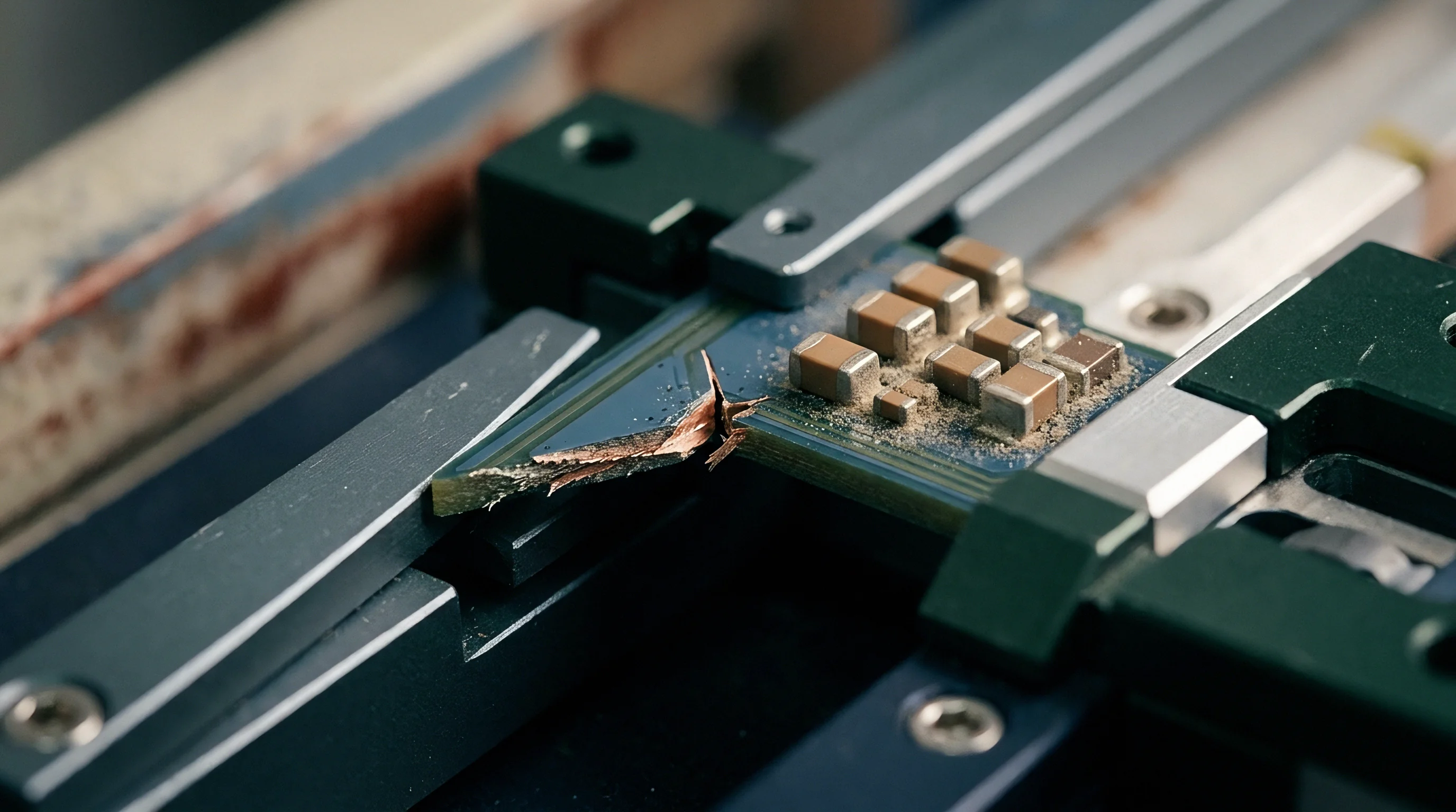
Hybrid Dielectric Selections and Fiber Weave Dispersion
Standard laminates consist of woven fiberglass fabric embedded in epoxy resin. Common styles such as 1080 or 7628 have noticeable gaps between yarn bundles where resin pools. The resin dielectric constant sits near 3.0, whereas the glass yarn measures around 6.0.
An RF trace running directly over a glass bundle encounters a higher dielectric constant than an identical line positioned over a resin-rich window. That variation skews phase velocities across multi-channel antenna routes, degrading beamforming accuracy and MIMO spatial diversity.
| Material Class | Dielectric Constant (1 GHz) | Loss Tangent (1 GHz) | Glass Styles | Relative Substrate Cost |
|---|---|---|---|---|
| Standard FR-4 | 4.2 to 4.7 | 0.020 | 1080, 2116, 7628 | 1.0x baseline |
| High-Tg FR-4 | 3.9 to 4.3 | 0.015 | 1080, 2116, 3313 | 1.2x baseline |
| Panasonic Megtron 6 | 3.7 | 0.002 | 1035, 1078 (Spread) | 2.5x baseline |
| Rogers RO4003C | 3.38 | 0.0027 | Woven Glass / Ceramic | 4.5x baseline |
Specifying spread-glass styles like 1035 or 1078 requires suppliers to use flattened glass yarns with minimal window gaps. Spread glass evens out the dielectric constant across the laminate, maintaining phase alignment across antenna feed networks.
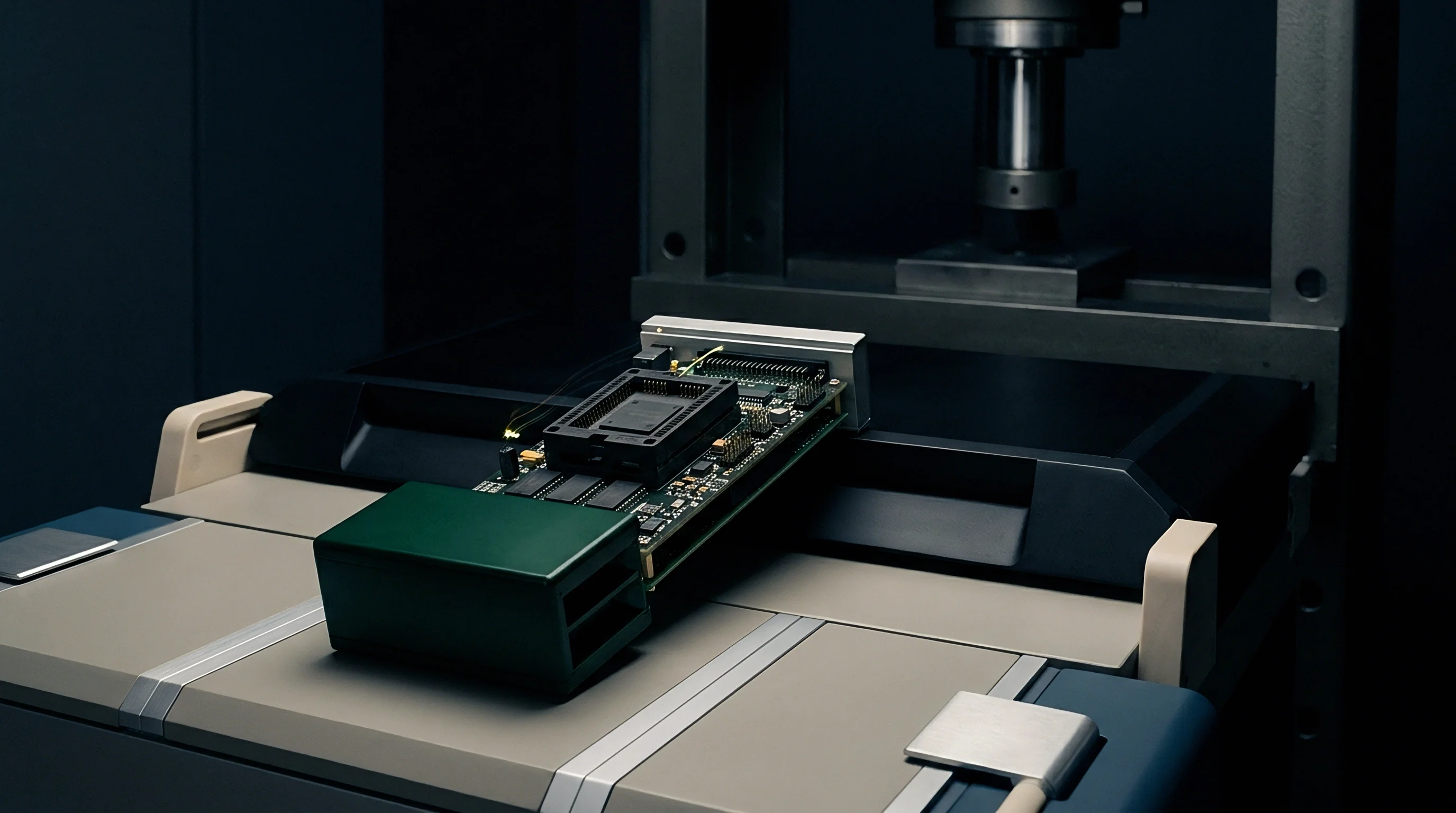
Panel Routing Depanelization Stress and RF Trace Integrity
Volume production requires stepping individual board designs into multi-up fabrication panels. Common separation methods include V-scoring and tab routing with perforated breakaway tabs. The mechanical load during breakout introduces microcracks in surface-mount ceramic components and solder joints beneath radio modules.
V-scoring exerts severe shear stress along the score line. Placing RF matching inductors or ceramic chip antennas within 2.5 mm of a V-groove leads to cracked ceramic bodies or severed solder joints during manual panel separation.
Placing passive matching components within three millimeters of a breakaway tab-routing line exposes surface mount terminations to mechanical flexure levels exceeding 750 microstrain.
Routing profiles should maintain at least 3.0 mm of clearance from all RF module pins and ceramic passives. Tab routing with laser-cut tabs avoids mechanical breakout stress on dense wireless designs.
Uneven copper distribution between internal layers causes panel warpage during reflow. Asymmetrical copper balance causes thin host boards to bow, preventing surface-mount wireless module pads from making full contact across flat stencil solder deposits.
Symmetrical layer stackups prevent panel twisting during high-temperature lead-free reflow operations.


Dossier
Handoff of a manufacturing package to a contract manufacturer requires systematic validation across all mechanical, electrical, and optical files. A missing Gerber layer or outdated drill table halts the factory line or prompts CAM edits that introduce latent defects.
A production release package must bundle raw design files with derived manufacturing outputs to allow independent audits and automated netlist cross-checks.

Fab Package Handover and Netlist Verification Rules
Electrical testing of bare boards relies on an IPC-D-356 netlist exported directly from schematic capture. This format lists electrical connections by net name, pin assignment, hole size, and coordinate location.
During tooling setup, CAM software extracts a separate netlist from the Gerber artwork. Comparing the schematic-derived IPC-D-356 netlist against the Gerber-derived artwork netlist flags layout export errors, such as inverted plane polarities that short power rails directly to ground.
The list below defines essential deliverables required in a fully validated wireless design transfer package.
- Schematic IPC-D-356 Netlist provides the authoritative reference netlist for automated bare-board continuity and isolation testing on the factory floor.
- Intelligent Artwork Files containing IPC-2581 or ODB++ datasets deliver complete stackup geometry, layer function tags, and trace impedance targets in a unified format.
- RS-274X Gerber Sets supplied as legacy fallbacks must include explicit layer identification naming conventions and complete solder mask and stencil aperture layers.
- Excellon NC Drill Files detailing plated, non-plated, blind, microvia, and backdrilled hole coordinates alongside precise tool sizing tables.
- Master Fabrication Drawing defining IPC performance class, solder mask color, surface finish specs, impedance tolerance bands, and board warp limits in PDF format.
- Centroid Pick and Place Data defining component reference designators, X-Y pad centers, rotation angles, and board origin offsets for automated SMT placement machinery.
Auditing the bill of materials against CAD land patterns avoids footprint mismatches during assembly. RF matching circuits using 0201 or 01005 discrete passives require component package sizes to match the exact solder pad geometry exported in the copper layers.

Bill of Materials Matching and Passives Tolerances
Selecting RF matching passives demands strict attention to component parasitic properties, self-resonant frequencies, and component tolerances. Swapping a 1.0 pF capacitor for an alternate part with the same nominal value but a lower self-resonant frequency detunes the matching network, reflecting RF energy back into the transmitter output stage.
During the transition of a 2.4 GHz custom radio board from prototype fabrication to volume production, the initial archive contained Gerber files, a bill of materials spreadsheet, and a schematic PDF. CAM intake scripts at the contract manufacturer compared the schematic netlist against the exported Gerber artwork, triggering an immediate mismatch error.
The log identified three net discrepancies around the radio module RF output pin. Net RF_OUT tied pad 1 of inductor L1 to the module in the schematic netlist, but the Gerber copper trace contained a 0.05 mm gap caused by an automated keep-out around an adjacent thermal via. Without the IPC-D-356 netlist comparison, production would have proceeded with an open circuit on the primary antenna line across the entire build.
Resolving the discrepancy required adjusting the clearance rule in the native CAD tool and re-exporting the artwork layers, resulting in a two-day schedule slip and a 450 USD CAM re-submission charge.
Bypassing automated netlist verification during data handoff leaves subtle geometry and routing shifts completely uninspected prior to fabrication tooling.


Invoice
Fabrication pricing for wireless host boards is driven largely by drawing tolerance callouts. Specifying non-standard limits on trace widths, layer thicknesses, and hole registration lowers factory yield, which suppliers absorb by adding risk surcharges to piece-part quotes.
Baseline IPC Class 2 tolerances allow factories to maintain high throughput with standard process controls. Stepping up to IPC Class 3 or imposing narrow impedance windows increases unit pricing while introducing additional inspection steps.
Yield Loss Factors and Non Recurring Engineering Surcharges
Impedance requirements are a primary driver of non-recurring engineering charges and unit pricing. Standard processing holds a plus or minus 10 percent impedance tolerance on microstrip and coplanar lines without degrading scrap rates.
Tightening impedance to plus or minus 5 percent requires coupon testing on every production panel, active tuning of prepreg press cycles, and scrapping panels that drift outside the target window. Those measures can double or triple bare-board unit costs.
| Design Parameter | Standard Tolerance (IPC Class 2) | Tight Tolerance (High Cost) | Bare Board Cost Impact |
|---|---|---|---|
| Controlled Impedance | +/- 10% | +/- 5% | 1.3x to 1.8x base price |
| Dielectric Height | +/- 10% | +/- 5% | 1.2x to 1.5x base price |
| Drill Hole Registration | +/- 0.075 mm | +/- 0.038 mm | 1.2x base price |
| Surface Finish (ENIG vs HASL) | Lead-free HASL baseline | ENIG (Electroless Nickel Immersion Gold) | 1.15x to 1.35x base price |
| Board Profile Routing | +/- 0.13 mm | +/- 0.05 mm (Laser) | 1.4x base price |
Surface finish selection balances material cost against insertion loss and pad flatness. Lead-free HASL leaves uneven solder crowns on fine-pitch radio footprints, leading to component misalignment during placement. Electroless Nickel Immersion Gold provides the flat surface required by fine-pitch land grid arrays, but carries a chemical processing surcharge on the invoice.

CAM Modifications and Tolerancing Cost Multipliers
Board shops routinely run automated CAM scripts on incoming Gerber sets to improve manufacturing yields. Typical automated adjustments include widening solder mask openings, expanding pads to offset chemical etch undercut, and trimming trace edges near adjacent copper.
Unchecked CAM adjustments alter critical RF geometry without designer sign-off. A routine script that trims 0.015 mm off top-layer copper to prevent bridging on digital routing will simultaneously shift a 50 Ohm coplanar antenna line to 56 Ohms, degrading RF performance across the entire production lot.
Master fabrication drawings should include unambiguous notes prohibiting modifications to top-layer RF trace widths or ground gaps without written engineering approval. Constraining critical geometries in the CAM instructions maintains RF performance while keeping fabrication costs within scope.