Meaning
Power integrity distortions that occur when multiple output drivers transition at the same instant define the transient noise on a system’s power rails. This simultaneous switching noise is caused by the rapid change in current flowing through the parasitic inductances of the package and board. The resulting voltage fluctuations can cause logic errors or disrupt signal transmission on adjacent traces.
Parasitic Inductance
Package pins and bonding wires present an inductive path to the supply and ground currents. When many outputs switch together, the combined current transient creates a voltage drop across these parasitic inductors. This voltage drop is called ground bounce when it affects the ground rail, or power sag when it affects the supply rail.
Minimizing this parasitic inductance is essential for high-speed design.
Signal Integrity
Voltage fluctuations on the internal power rails can degrade the transitions of the output drivers, causing timing jitter. The noise can also propagate through quiet output lines, appearing as unwanted signal spikes at the receiver. These spikes can be mistaken for valid signal transitions by receiving gates.
Design margins must account for these noise sources under worst-case switching conditions.
Board Layout
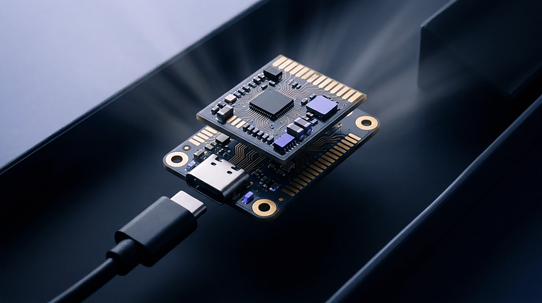
Designers reduce this noise by using multi-layer boards with dedicated ground and power planes. Placing decoupling capacitors close to the power pins provides a local source of current, reducing the transition flow through the package inductors. Using ball grid array packages instead of leaded packages also lowers the parasitic connection inductance.
Proper layout minimizes the noise generated during high-speed operations.