Meaning
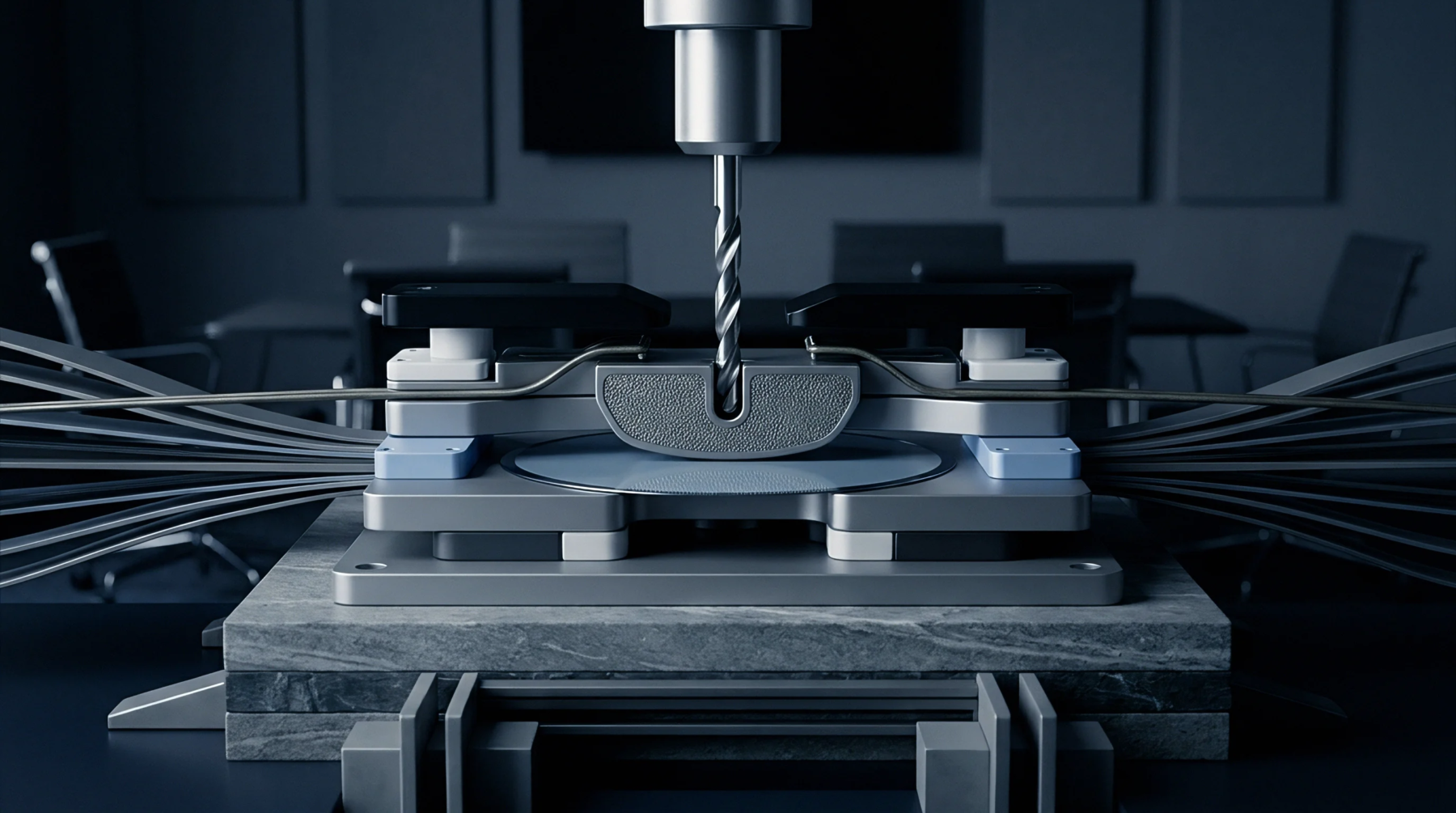
The division of a single production batch of semiconductor wafers into sub-batches during the manufacturing process enables controlled experimental testing. Fabrication engineers utilize a split lot to evaluate different process variations or materials under identical baseline conditions. This technique keeps the environmental and machine variables constant across all wafers, allowing for an accurate comparison of the modified parameter.
It provides empirical data to optimize transistor performance before full production begins.
Experimental Division
Wafers are separated at a specific manufacturing step to receive different exposure times or thermal treatments. A split lot might involve applying a new dielectric material to half of the wafers while the other half serves as the control group. This direct comparison isolates the effect of the process change.
Manufacturing Execution
Tracking systems in the foundry must monitor the individual sub-batches to ensure they are recombined or processed correctly in subsequent stages. Managing a split lot increases the complexity of production scheduling and routing within the cleanroom. This complexity requires automated recipe management.
Process Optimization
Analyzing the test data from each group reveals which processing conditions yield the best electrical performance. The split lot methodology reduces the time required to qualify new manufacturing equipment or processes. This testing accelerates the development of more efficient chips.