Meaning
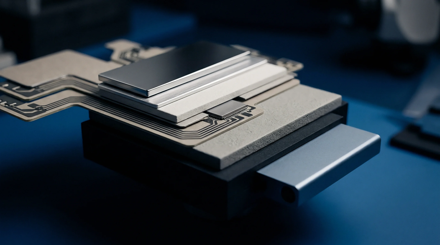
Center-to-center spacing dimensions between adjacent conductive copper traces on printed circuit board substrates define routing density and electrical isolation boundaries in high-density interconnect designs. Hardware design engineers specify substrate trace pitch to balance signal routing channel density against dielectric breakdown limits and cross-talk suppression in compact cellular modules. The geometric metric governs trace width and spacing combinations achievable by automated PCB photolithography and chemical etching processes.
Coupling Behavior
Placing high-speed digital traces or high-frequency radio signals in close proximity increases capacitive and inductive crosstalk across intervening substrate dielectric material. Tightening substrate trace pitch increases connection density beneath fine-pitch ball grid array components, but requires reduced signal voltage swings and differential routing strategies to maintain signal integrity. Layout engineers insert ground guard traces and specify precise dielectric thickness values when trace pitch drops below standard manufacturing guidelines.
Controlled dielectric properties prevent signal degradation across adjacent radio frequency lines.
Manufacturing Yield
Etching fine copper traces near substrate resolution boundaries increases the risk of micro-shorts caused by residual copper bridges or open circuits from over-etching. Narrow substrate trace pitch demands advanced high-density interconnect fabrication processes, including laser direct imaging and semi-additive processing. Substrate suppliers inspect fine-pitch trace layers using automated optical inspection equipment to catch copper defects prior to lamination.
Thermal Limit
High-current power traces require wider conductor spacing and thickness to dissipate heat without raising local board temperature. Narrow spacing limits continuous current capacity across power delivery networks.