Boundary Scan Chain Verification Protocols for Dense Assemblies
Boundary scan verification on dense assemblies requires strict TCK signal integrity, validated BSDL cell maps, and IEEE 1149.6 pulse testing for AC-coupled nets.


Node
When micro-BGA devices drop to ball pitches of 0.4 mm or narrower on dense boards, over eighty percent of circuit nets lose physical probe access entirely. Substrate fan-outs leave no room to land test pads, and standard bed-of-nails fixtures with spring-loaded pogo pins cannot contact high-density interconnect traces without risking mechanical damage or introducing intolerable capacitive loads. IEEE 1149.1 boundary scan gets around this physical barrier by shifting test data serially through dedicated shift-register cells integrated directly into compliant silicon.
Chain stability across a multi-layer board depends on Test Access Port signal integrity. The four-wire physical interface ~ Test Clock, Test Mode Select, Test Data In, and Test Data Out ~ must hold up across dozens of compliant parts, which makes Test Clock routing especially sensitive to transmission line effects. Signal reflections or ground bounce on clock traces can double-clock the TAP controller’s internal state machine, kicking it prematurely out of Shift-DR and into Exit1-DR.
Signal skew halts the test sequence outright, while clean clock distribution prevents diagnosing phantom opens.

Signal Routing for High Speed Test Access Ports
Daisychaining Test Data Out to Test Data In across forty or fifty complex ICs introduces substantial trace delay and signal distortion. To prevent edge degradation on high-density interconnect designs, Test Clock is distributed as a point-to-multi-point buffered tree. Because propagation delay still mounts over long routes, low-skew clock buffers are inserted to keep clock transitions aligned at every TAP controller in the boundary scan chain.
Test Mode Select lines require identical path length matching to prevent individual silicon state machines from desynchronizing during shift operations.
| Substrate Technology | Max TCK Frequency (MHz) | Max TAP Chain Length (Devices) | Trace Impedance Target (Ohms) | Termination Requirement |
|---|---|---|---|---|
| Standard FR4 (4-Layer) | 10 to 25 | 32 | 50 ± 10% | Parallel AC at Chain End |
| High-Density Interconnect (12-Layer Micro-via) | 25 to 50 | 16 | 50 ± 5% | Series Source + AC Parallel |
| Silicon Interposer (2.5D System-in-Package) | 50 to 100 | 8 | 45 ± 3% | On-Die Termination (ODT) |

Substrate Impedance and Clock Distribution Dynamics
Trace impedance shifts abruptly across micro-via transitions within the substrate stack-up. A 50-ohm trace entering an inner-layer micro-via array encounters localized capacitance drops where ground reference planes are removed beneath dense ball fields. The resulting capacitance shift rounds clock edges, extending rise times past the two-nanosecond threshold required by modern high-speed boundary scan controllers.
Placing low-capacitance Schottky diode clamps near the final receiver pin dampens voltage ringing caused by line stubs.
Single-ended clock trees require active termination whenever trace propagation delay exceeds half the clock signal rise time.
IEEE 1149.7 multi-drop architectures reduce overall line count and allow test routines to isolate failing silicon segments without dropping the entire scan path. In a legacy IEEE 1149.1 chain, a single open Test Data In bond wire or a shorted internal shift cell breaks serial continuity entirely. Star and shadow-protocol topologies let automated test stations bypass unpopulated or damaged devices, keeping verification access intact across adjacent functional components.
TAP signal interconnects demand the same high-frequency layout rigor applied to high-speed synchronous data buses to prevent transient switching noise from invalidating manufacturing test sweeps.


Parsing
EDA toolchains synthesize structural test vectors directly from component Boundary Scan Description Language files published by IC manufacturers. If a BSDL file contains syntax errors or inaccurate boundary cell register assignments, the toolchain generates flawed patterns that produce false failures or overlook solder bridges. Given how frequently vendor files contain instruction typos, automated parsing requires rigorous sanity checks.

Syntax Validation and Cell Mapping Verification
Pre-synthesis syntactic validation enforces strict compliance with IEEE 1149.1 BSDL rules before vector synthesis begins. Parser engines verify the exact bit length of the Instruction Register, the binary opcodes for mandatory instructions including EXTEST, SAMPLE/PRELOAD, and BYPASS, and the pin-to-cell mapping table. Discrepancies between the physical package pinout map and internal boundary register definitions frequently emerge when silicon vendors revise package hardware without incrementing the BSDL file version control tag.
- Instruction Register Register Length Verification confirms the precise shift count needed to load opcodes without corrupting adjacent silicon state machines in the chain.
- Pin Boundary Cell Type Audit checks whether dedicated input, output, or bidirectional cells match the operational hardware capabilities of the physical silicon pad.
- Safe State Vector Definition validates that control cells default to inactive states during EXTEST execution, preventing bus contention between active drivers on shared parallel traces.
- IDCODE and USERCODE Register Alignment matches thirty-two bit hardcoded vendor device identification codes against physical silicon readbacks during initial chain discovery.
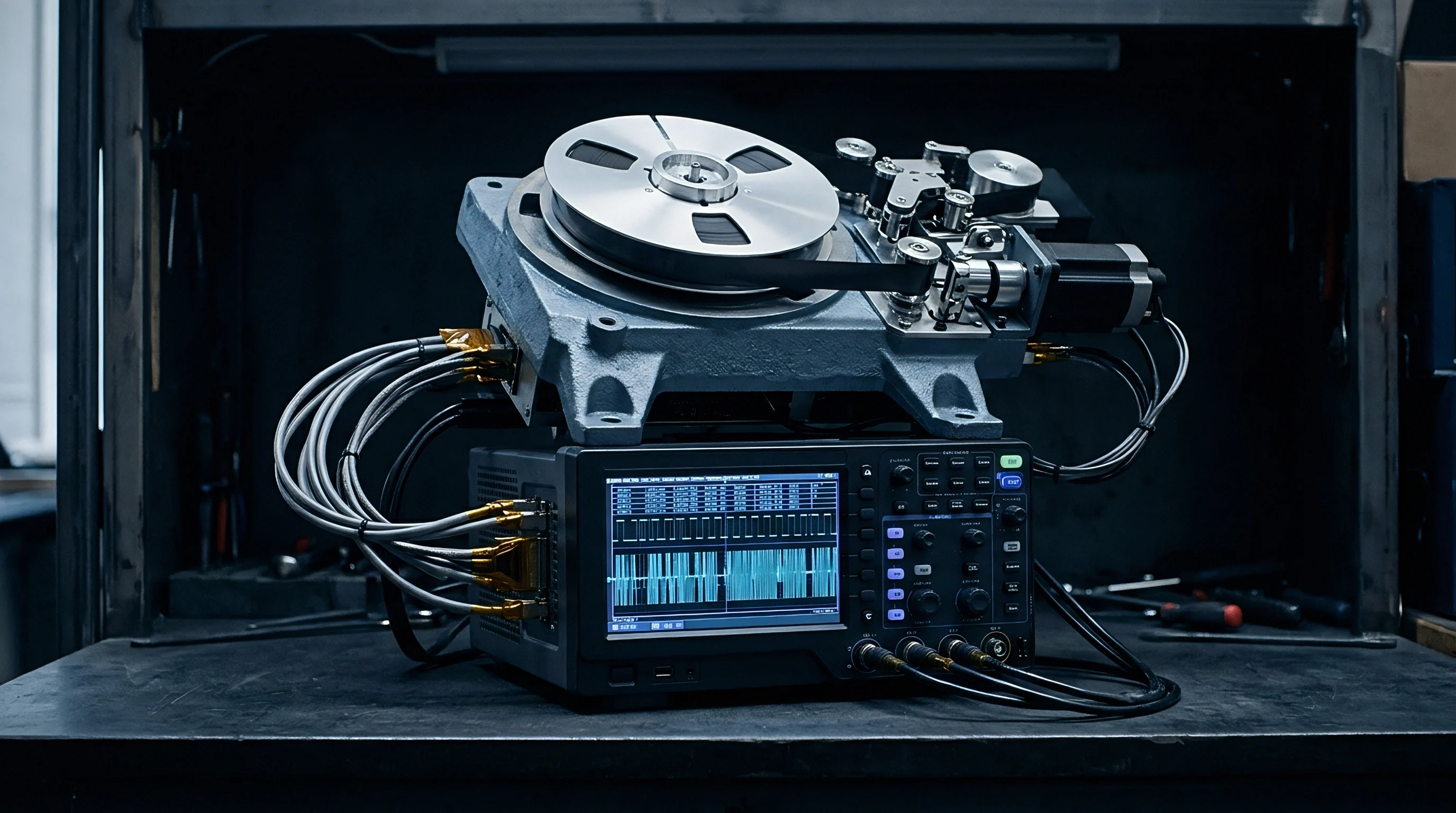
Silicon Revisions and Undocumented Register Shifts
Die shrink operations and stepping revisions change internal boundary scan cell order. A BSDL file written for revision A silicon will shift data into incorrect boundary cells when loaded onto revision B hardware, applying output voltages to input-only pins or disabling output drivers during structural interconnect tests. Loading unverified model files into automated test fixtures routinely corrupts test vectors and breaks factory runs.
Published BSDL files frequently pass standard IEEE parser checks yet still require benchtop validation against live hardware before release to production test benches.


Coupling
High-speed differential serial links operating above five gigabits per second rely on series AC coupling capacitors that block traditional direct-current boundary scan operations. Because standard IEEE 1149.1 EXTEST patterns apply static DC voltage levels to evaluate continuity, series capacitors prevent current flow, leaving conventional boundary scan cells incapable of detecting open circuits or shorted traces on PCIe Gen 4, SAS, or Ethernet physical layers.

IEEE 1149.6 Edge Control and Pulse Generation
IEEE 1149.6 addresses AC-coupled and differential networks by introducing specialized boundary scan cell architectures capable of generating and receiving transient voltage transitions. AC EXTEST instructions drive step functions or square wave pulse trains across high-speed channels. The transmitter boundary cell converts static shift register bits into high-frequency edge pulses, while receiver cells incorporate hysteresis elements and memory latches to detect step transitions through series capacitance values ranging from 10 to 200 nanofarads.
- Initialize Advanced Boundary Cells by shifting the EXTEST_PULSE opcode into the Instruction Registers of all IEEE 1149.6 compliant ICs along the differential link path.
- Load Dynamic Preload Patterns into the Data Registers to establish initial differential voltage polarity across the transmit drivers.
- Execute Step Edge Injection by cycling Test Clock, triggering internal pulse generators that send positive-going and negative-going voltage steps through the coupling capacitors.
- Latch Receiver Hysteresis Output into the destination boundary cell during the Capture-DR state of the TAP controller.
- Shift Results Out Serially through TDO to analyze step response amplitudes and identify broken differential pairs or shorted capacitor pads.

Differential Signal Verification across AC Capacitors
Differential signaling requires receiver cells to evaluate both true and complement signal lines simultaneously. An open circuit on one arm of a differential pair degrades signal margin and allows single-ended crosstalk to trigger false passes in receiver logic. To verify these paths, IEEE 1149.6 vector suites run differential EXTEST_TRAIN sequences, using repeating pulse patterns that force receiver cells to measure differential step height and common-mode voltage offsets.
IEEE 1149.6 Clause 6.2 mandates that receiver boundary cells detect step transitions down to a minimum threshold of 50 millivolts peak-to-peak across capacitive isolation barriers.
Under commercial assembly contracts referencing IPC-A-610 Class 3 acceptance criteria, test reports generated via unvalidated IEEE 1149.6 vector chains do not constitute proof of structural interconnect compliance for AC-coupled high-speed interfaces.


Scoping
Test coverage calculations for high-density assemblies determine whether incoming inspection catches manufacturing defects prior to final encapsulation. Because dense assemblies eliminate physical test points, traditional in-circuit test models become ineffective for coverage verification. Quality teams turn to the PCOLA-SOQ model to quantify component-level and interconnect-level fault protection across Presence, Correctness, Orientation, Live performance, Alignment, Short circuits, Open circuits, and Quality metrics.

Structural Coverage Accounting via Boundary Vectors
Boundary scan vectors evaluate interconnect nets bounded by compliant silicon boundary cells. Non-compliant components, including passive resistor networks, discrete transistors, and legacy analog ICs, reduce structural coverage unless cluster testing protocols bridge the boundary gap. Cluster testing uses surrounding compliant IC boundary cells to drive stimulus patterns through non-compliant passive networks, reading back response values on adjacent boundary-compliant inputs.
| Test Methodology | Physical Test Access Needed | Interconnect Open Coverage | Interconnect Short Coverage | Average Cycle Time per Board |
|---|---|---|---|---|
| In-Circuit Test (Bed-of-Nails) | 100% Net Physical Access | 98% | 99% | 8 to 15 Seconds |
| Standard IEEE 1149.1 Scan | TAP Header Pins Only | 72% | 85% | 12 to 30 Seconds |
| Hybrid IEEE 1149.1/1149.6 + Cluster | TAP Header + 5% Edge Access | 94% | 96% | 20 to 45 Seconds |
| Flying Probe Testing | 80% Net Physical Access | 95% | 97% | 180 to 450 Seconds |

Vector Density and Scan Time Arithmetic
Evaluating test duration requires balancing serial vector shift depth against Test Clock frequency limits. A mainboard carrying four large FPGAs, two system-on-chip processors, and six DDR memory controllers on a single boundary scan chain illustrates how scan depth accumulates where physical test pads are absent.
Assume the combined boundary register length across all devices totals 24,500 boundary cells. A comprehensive interconnect fault pattern suite for a board with 3,200 unique circuit nets requires executing modified counting algorithms to isolate bridging shorts. The vector calculation uses the binary log of the net count plus shift overhead buffers.
Total patterns required equal 12 short-isolation vectors plus 24 open-detection vectors, giving 36 distinct test frames. Shifting 24,500 bits per pattern 36 times demands 882,000 clock cycles. At a conservative TCK operational frequency of 10 MHz (100 nanoseconds per clock period), pure serial shift time takes 88.2 milliseconds.
Adding TAP controller state transition overhead, memory buffer reloads, and diagnostic readback shifts increases overall boundary execution time to 1.45 seconds per assembly.
When automated test scripts add cluster testing for non-boundary memory chips connected to processor buses, vector bit depth escalates rapidly. Driving 100,000 write-read test patterns through boundary cells into external parallel NOR flash memory to verify address and data line continuity shifts 2.45 billion bits serially. At 10 MHz TCK, memory cluster verification inflates execution time to 245 seconds.
This cycle time penalty forces test engineers to shift memory structural testing from boundary scan EXTEST routines to functional bootloader execution, trading structural fault isolation accuracy for factory line throughput speed.
A boundary scan chain containing 24,500 cells operating at 10 MHz TCK requires 1.45 seconds for structural interconnect verification, but cluster memory testing expands execution time to 245 seconds.
Omission of structural boundary verification for high-density BGA interconnects shifts manufacturing defect discovery from incoming board assembly lines to final functional systems integration, escalating repair costs by a factor of ten for every test stage bypassed.


Diagnostics
Fault isolation algorithms process raw scan register output patterns to pinpoint open solder joints, bridging shorts, and missing silicon dies. When a boundary scan vector set fails, the automated test environment extracts the miscompared bit positions from the captured Shift-DR stream. By cross-referencing failing bit positions against the master BSDL netlist, the diagnostic engine maps serial bit offsets back to physical IC package pins and circuit board trace identifiers.

Where Do Boundary Scan Vectors Fail on Dense Interconnects?
Vector failures cluster around high-density fine-pitch components where solder bridging and head-in-pillow defects dominate manufacturing yield losses. Head-in-pillow defects create intermittent mechanical contact between the BGA solder ball and the printed circuit board pad, passing room-temperature continuity tests but failing under thermal stress. Boundary scan EXTEST vectors executed inside environmental stress screening chambers catch these intermittent opens by applying continuous parallel patterns during thermal cycling.
Higher trace resistance introduced by micro-vias narrows receiver timing margins, demanding precise edge placement during high-speed diagnostic sweeps.

Hybrid Test Systems Combining Scan with Flying Probes
Integrating boundary scan software engines with automated flying probe hardware bridges the coverage gap on nets lacking compliant boundary cells. Flying probe needles contact accessible edge connectors or decoupling capacitor pads, acting as dynamic stimulus points while internal boundary scan cells capture forced voltage states on compliant IC inputs.
Executing an integrated hybrid diagnostic routine follows a strict operational sequence to isolate complex structural faults without damaging sensitive low-voltage silicon pads.
- The flying probe system executes a net resistance check to confirm proper grounding across all board power rails before applying active power.
- System power turns on, and the boundary scan controller issues a TAP reset command to force all internal TAP state machines into the Test-Logic-Reset state.
- The boundary scan software loads the BYPASS instruction across all chain devices to confirm serial TDI-to-TDO continuity and verify chain integrity.
- Boundary scan EXTEST patterns initialize compliant IC output cells to high-impedance states, preventing driver contention during probe contact.
- The flying probe needle deposits a programmed current pulse onto a non-boundary target trace while adjacent boundary cells capture incoming logic levels.
- The diagnostic software compares captured boundary shift data against netlist topology matrices to pinpoint exact failure coordinates down to a single BGA pad.
| Fault Condition | Primary Detection Vector | Diagnostic Isolation Resolution | False Positive Rate |
|---|---|---|---|
| Single Pin Open (Compliant Net) | EXTEST Walking 1s / 0s | Exact IC Pin and Net ID | Under 0.1% |
| BGA Solder Bridge (Adjacent Nets) | Modified Counting Algorithm | Exact Net Pair Identification | Under 0.5% |
| Head-in-Pillow Intermittent Open | Thermal Cycle EXTEST Loop | Specific IC Pin (Requires Thermal Stress) | 2.4% |
| Non-Compliant Pass-Through Short | Hybrid Boundary Scan + Flying Probe | Component Level Circuit Stub | 4.1% |
Pin-level diagnostic resolution remains unverified when micro-BGA packages incorporate internal sub-stack silicon interposers that bypass the primary boundary scan chain.


Escrow
Intellectual property ownership bound to boundary scan assets defines whether a buyer can transfer board manufacturing between alternative assembly houses. Turnkey manufacturing contracts often leave test pattern source files, custom BSDL hardware mappings, and diagnostic dictionary databases in the hands of the primary contract manufacturer. Transferring assembly operations without securing complete vector source files obligates the buyer to repurchase boundary scan engineering development from scratch.

Test Pattern Deliverable Formats and Target Execution Engines
Vendor-neutral boundary scan deliverables rely on standardized vector file formats to maintain cross-platform compatibility. Serial Vector Format (SVF) files and Standard Test and Programming Language (STAPL) files record boundary scan state transitions, shift patterns, and expected readback values in plain text human-readable formats. Delivering raw SVF or STAPL files allows secondary manufacturing sites to execute verification suites on automated test platforms from any vendor.
A complete design handover package includes validated component BSDL files, original CAD netlists formatted in IPC-2581 or GenCAD, compiled test execution binaries, and source-level SVF/STAPL files for all interconnect and programming routines.

Vendor Contractual Scope for Boundary Verification Package
Statements of work must explicitly state ownership transfer terms for boundary scan test development assets. Non-Recurring Engineering (NRE) fees billed by assembly vendors for test development cover BSDL file validation, netlist topology extraction, test vector synthesis, structural coverage reporting, and fault dictionary generation. Standard engineering contracts assign output file copyright to the buyer upon final payment of NRE line items.
Complete boundary scan handover packages require plain-text SVF or STAPL vector sources alongside original BSDL hardware definition files to enable platform-independent test execution.
Contractual scope definitions specify that boundary scan integration packages pass acceptance testing using an independent target execution engine prior to final invoice settlement. The factory provides full coverage breakdown dossiers detailing unverified nets, physical access limitations, and isolated cluster fault boundaries, transferring full operational custody of the structural verification suite to the client engineering team.