Defining Core Ownership Boundaries in Module Circuit Schematic Transfer
Define explicit native CAD deliverables and test fixture ownership in engineering scope contracts to ensure seamless secondary manufacturing transfer.


Stack
Architectural decisions in wireless and processing modules establish distinct tiers of design visibility. The chosen integration depth dictates whether an engineering team receives full circuit visibility, limited interface schematics, or an encrypted black-box hardware block. Sourcing practice classifies these tiers into turnkey modules, semi-custom reference derivatives, custom white-label assemblies, and full technology transfer packages.
Each tier shifts technical debt and design ownership between module supplier and host integrator.
Turnkey procurement assigns complete circuit responsibility to the vendor while shielding original IP. System integrators obtain block diagrams and pinout definitions, sufficient for footprint placement on a host printed circuit board. The internal schematic remains locked within the vendor’s domain.
Semi-custom arrangements permit selective modifications, such as adjusting power management ICs or optimizing RF front-end filtering. Under semi-custom scope, the vendor supplies partial schematics covering host interface pins and peripheral passive networks while withholding baseband core schematics.
Modules reduce initial capital expenditures. Custom white-label programs invert this dynamic by paying non-recurring engineering fees to build a proprietary hardware footprint. The vendor designs the circuit to host specifications, but ownership terms govern whether native schematic files transfer upon program completion.
Full technology transfer represents the complete handover of raw EDA databases, allowing independent manufacturing at third-party contract facilities.
| Integration Level | Schematic Transfer Scope | IP Ownership Boundary | Layout Modification Freedom | Second-Source Rights |
|---|---|---|---|---|
| Turnkey Standard | Flat PDF interface drawing only | 100% Vendor proprietary | Zero modification allowed | Prohibited |
| Semi-Custom Derivative | Partial EDA schematics for IO blocks | Shared core IC vendor, host IO | Host peripheral nodes only | Restricted to approved CMs |
| Custom White-Label | Complete native schematic CAD database | Host owns board netlist IP | Full control over layout revision | Permitted via licensing fee |
| Technology Transfer | Full EDA source, symbol libraries, netlists | Host owns complete schematic design | Unrestricted layout modification | Fully assignable without fee |
Contractual scope defines whether a customer receives editable native schematics or flat PDF drawings. Flat drawings serve host integration but prevent component re-annotation or signal path re-routing. When an engineering team attempts to migrate a module from an established vendor to a lower-cost manufacturing partner without native CAD sources, design continuity collapses.
Layout engineers must reverse-engineer net connectivity, introducing signal integrity risks and extending time-to-market.
Unclear integration terms expose host applications to sudden single-source lock-in. When a silicon component within a turnkey module faces end-of-life status, the module manufacturer dictates the replacement schedule and price adjustment. Integrators lacking internal schematic visibility cannot swap passives or adapt host firmware to alternative silicon revisions independently, leaving the host product vulnerable to component phase-outs.

Paperwork
Documentation packages transferred across company boundaries dictate whether a host platform can be manufactured independently. A schematic transfer requires comprehensive CAD databases rather than simple image exports. Gerber files convey zero intelligence.
Transferring Gerber artwork provides vector shapes for copper, silkscreen, and solder mask layers, but strips net names, component attributes, pin functions, and parametric constraints. CAD databases demand explicit licensing.
Schematic files distributed solely in PDF format freeze design revisions within the customer organisation. PDF drawings allow visual inspection of pin connections, yet host engineers cannot perform netlist extraction or automated electrical rules checks against their host board design. Complete transfer packages deliver native schematic project files created in industry-standard software, including associated component libraries, footprint cross-references, and parameter mapping tables.
CAD translation errors frequently alter pin types during conversion between design tools, creating silent open circuits or inverted logic levels.
IPC-2581 mandates complete XML-based circuit hierarchy and netlist definitions to prevent fabrication ambiguity during vendor handoffs.
Hardware schematics connect directly to software registers through micro-controller signal names and pin assignments. The schematic transfer package includes complete pin-mapping documentation detailing multiplexed functions, pull-up resistor defaults, and voltage tolerances. When pin functions are left undocumented, firmware engineers misconfigure internal microcontroller registers, causing bus contention or uninitialized floating inputs that drain battery reserves.
- Native Schematic Source Files formatted in EDA database formats allow host engineers to edit net connections and pin assignments.
- Custom Symbol Libraries containing parametric component attributes prevent missing component errors during local CAD compilation.
- Hierarchical Netlists exported in standard board format confirm complete connectivity between system blocks.
- Bill of Materials Database matching specific manufacturer part numbers guarantees component sourcing parity.
- Constraint Management Files defining high-speed routing rules and differential pair impedances maintain RF signal integrity.
Software development kits rely on board support packages hardcoded to specific schematic pinouts. Transferring hardware schematics without corresponding source code configuration headers leaves host developers unable to recompile firmware for derivative boards. The engineering scope agreement specifies whether hardware abstraction layer definitions, pin assignment header files, and peripheral driver source files accompany the physical circuit schematics.
Standard IP transfer agreements establish clear rights regarding secondary design derivation. Contracts specifying complete design handover incorporate explicit clauses that assign all netlist copyrights, symbol library assets, and associated layout constraint logic to the receiving entity upon final payment milestone sign-off.

Fixture
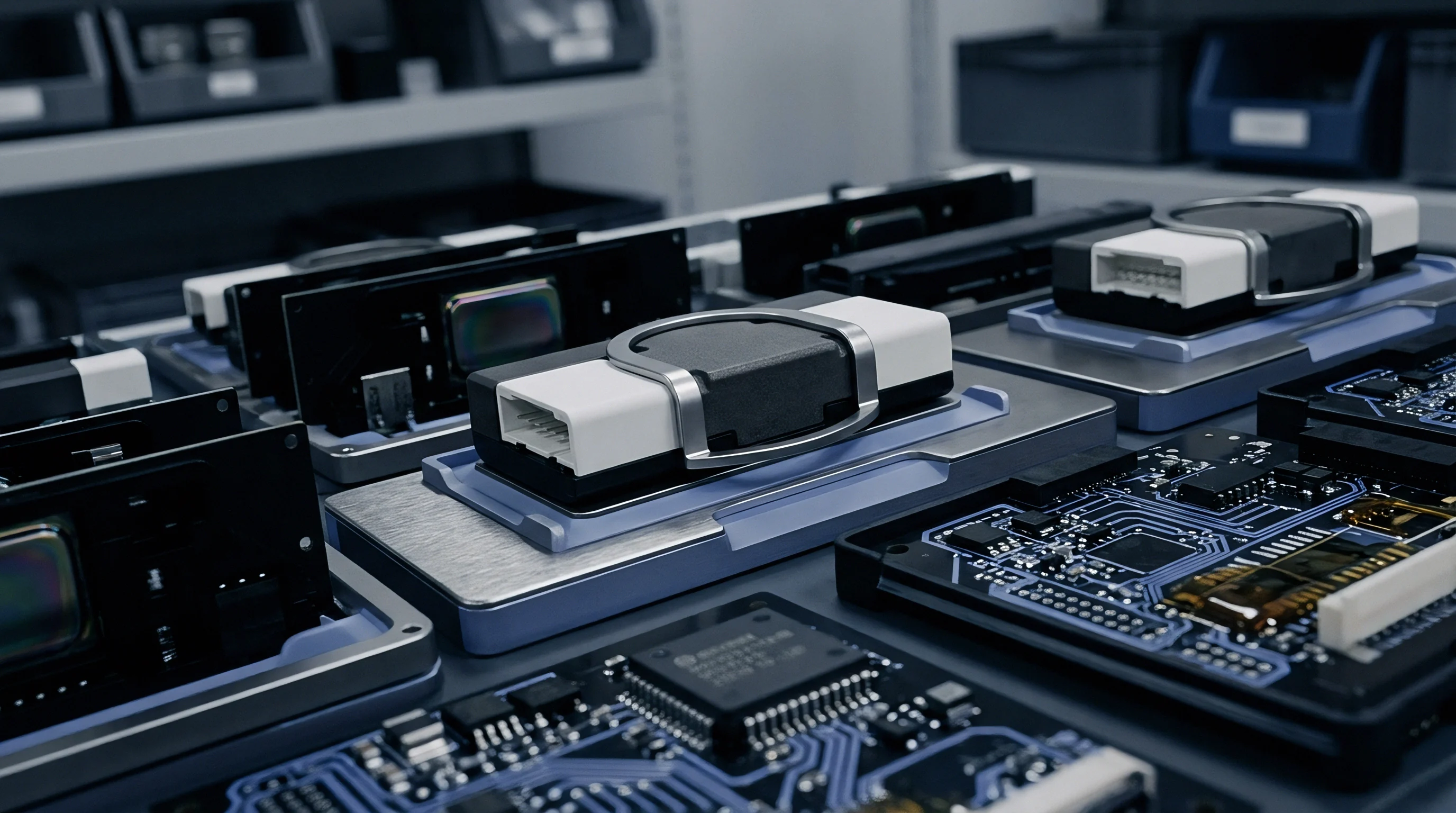
Factory acceptance relies on physical test rigs that validate raw board integrity and RF calibration. A design transfer that omits factory test schematics leaves the host customer unable to verify incoming build quality. Test jigs incorporate bed-of-nails pogo pin receivers, power supply sequencing circuits, signal conditioning amplifiers, and boundary scan interfaces.
Physical test fixtures carry costs.

Where Does Test Hardware Ownership Stop during Manufacturing Handover?
Boundary scan files and bed-of-nails pin assignments bridge the gap between module design and production testing. The physical test fixture schematic details how test pads connect to instrumentation channels, multiplexers, and load banks. Vendor turnkey quotes frequently exclude test fixture schematics, retaining ownership of the factory production line hardware.
When shifting manufacturing to a second-source factory, the buyer must duplicate the fixture hardware or pay the original vendor for fixture design release.
Factory test coverage drops rapidly when transferred schematic packages omit physical test point coordinates.
Automated test routines store trim factors and gain adjustments directly inside non-volatile memory registers. Transferred schematics specify crystal oscillator loading capacitors and RF matching components, but optimal operating points depend on software trim values calculated during factory test. Without access to the test bench schematic and associated calibration software, secondary factories cannot program precise frequency offsets or power amplifier bias limits into production units.
- Extract netlist connectivity files from source CAD schematics to verify pin assignment mapping against test software drivers.
- Run boundary scan vectors across all accessible interface nodes to confirm physical interconnect integrity on prototype hardware.
- Execute automated calibration algorithms on factory test fixtures while recording trim parameters into non-volatile storage.
- Compare golden sample measurement outputs against secondary manufacturing test logs to confirm specification alignment.
Testing uncovers assembly variations across production lots. When host engineers request full schematic transfer to establish a second manufacturing source, suppliers often cite proprietary test routine IP to restrict access to factory calibration code. The supplier claims that opening test scripts reveals trade secrets regarding silicon binning and yield optimization techniques.

Arithmetic
Commercial valuation of schematic ownership determines long-term module margins and total cost of ownership. Non-recurring engineering fees pay for upfront design hours, prototyping runs, and regulatory compliance testing. Standard non-recurring engineering agreements grant the buyer exclusive purchasing rights to the finished module but reserve underlying schematic IP ownership to the vendor.
Purchasing full schematic ownership requires an additional IP release fee or an elevated initial engineering charge.
Upfront payments covering schematic transfer divide sharply into non-exclusive design usage rights and full patent assignments. Non-exclusive rights permit the buyer to manufacture the exact schematic at alternative factories while restricting derivative modifications. Full assignment transfers total intellectual property rights, enabling the buyer to integrate module schematic blocks into larger system-on-chip or system-in-package designs without royalty obligations.
| Volume Tier (Units/Year) | Turnkey Unit Cost ($) | Buyout Amortized Unit Cost ($) | NRE & IP Buyout Expense ($) | Landed Cost Advantage |
|---|---|---|---|---|
| 10,000 | 28.50 | 42.00 | 135,000 | Turnkey preferred |
| 50,000 | 24.00 | 23.70 | 135,000 | Parity threshold |
| 100,000 | 22.10 | 17.85 | 135,000 | Schematic buyout preferred |
| 250,000 | 20.50 | 15.20 | 135,000 | Significant savings |
Consider a project requiring 100,000 wireless communication units per year over a four-year product lifecycle. A turnkey vendor quotes 22.10 dollars per module with zero upfront IP fee. An alternative semi-custom agreement charges 135,000 dollars in non-recurring engineering and IP buyout fees, but allows direct bill-of-materials sourcing at a unit manufacturing cost of 15.00 dollars plus a 2.85 dollar factory assembly fee, yielding 17.85 dollars per unit landed cost.
Over 400,000 cumulative units, total turnkey spend reaches 8,840,000 dollars, whereas the schematic buyout path totals 7,275,000 dollars including initial fees, generating a net saving of 1,565,000 dollars.
Full schematic ownership buyout yields positive financial returns at annual production volumes exceeding 75,000 units.
Second sources demand raw schematics. Unassigned pinouts break host hardware. Component obsolescence forces layout redesign.
Tooling amortisation alters landed economics. License grants determine modification rights. Netlist verification precedes layout execution.
High upfront NRE charges pay off only when production runs amortize intellectual property acquisition across high unit volumes.

Governance
Long-term maintenance of module designs requires disciplined engineering change routines across independent operational groups. Part-Change Notifications manage component substitutions caused by component end-of-life or supply chain shortages. When a vendor holds exclusive schematic ownership, they execute Engineering Change Orders unilaterally, updating passive values or silicon step revisions without host buyer approval as long as external form, fit, and function specifications remain constant.
Component obsolescence forces silicon replacements that alter pin electrical characteristics and RF tuning values. If the buyer owns transferred native schematics, internal hardware teams assume complete engineering change authority. The buyer must establish internal change review boards to qualify alternate passive components, verify modified RF matching netlists, and update fabrication master drawings.
Failure to maintain schematic revision control across second-source factories results in divergent hardware builds that behave inconsistently in the field.
Engineering change notifications without verified pin-mapping schematics create severe field failure exposure.
Hardware schematic revisions inevitably force changes in peripheral drivers and board initialization code. When a schematic transfer occurs, contract terms must define which party retains ongoing firmware patch obligations for newly introduced component revisions. If a host integrator modifies a transferred schematic to replace an obsolete power management IC, the original module supplier disclaims all warranty obligations and firmware maintenance support for that hardware variant.
- Unannounced Passive Component Substitutions shift RF matching network tuning and alter target emission compliance.
- Pin Assignment Mismatches cause driver initialization routines to trigger short circuits across host processor lines.
- Orphaned Firmware Drivers fail to initialize hardware features added during uncoordinated schematic revisions.
- Unsynchronized EOL Notifications force unexpected emergency redesign cycles when critical IC packages sunset.
Managing split responsibility across long product life cycles exposes structural friction between module design houses and product integrators. When field failures emerge on a modified second-source build, determining whether liability stems from the original vendor schematic design or the host integrator’s schematic alterations remains an open operational question.