Carrier Frequency Offset Mitigation in High Power Sub-GHz Transmitters
Mitigate sub-GHz transmitter frequency offset by isolating reference crystals from amplifier heat and buffering synthesizer tanks against antenna load pulling.

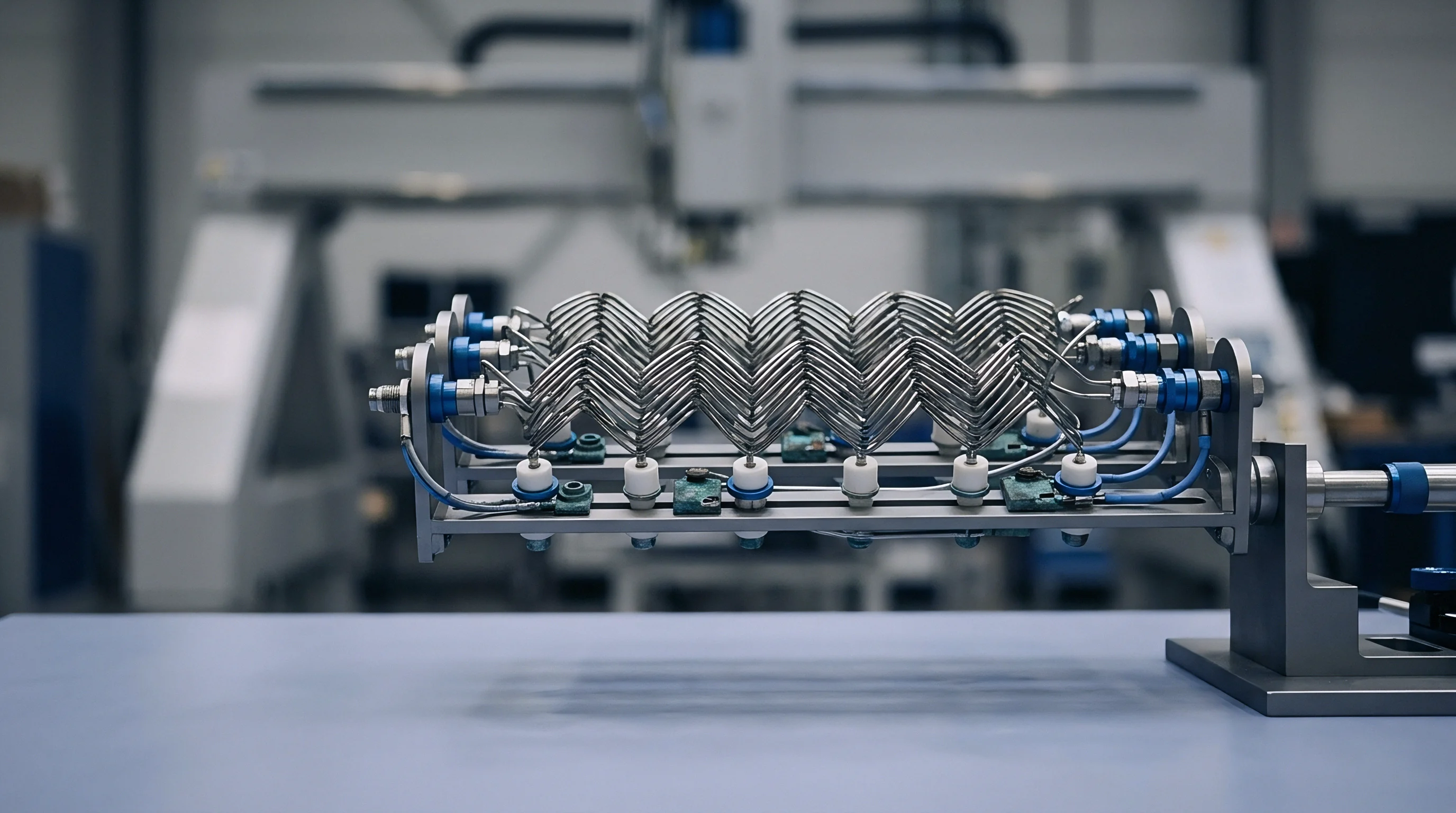
Shock
When a power amplifier operates above twenty-seven decibel-milliwatts, thermal gradients spread across the circuit board within milliseconds of turn-on. Surface-mount quartz crystals and TCXOs often sit only centimeters from silicon dumping three to five watts of heat. As that thermal pulse conducts through ground planes and copper traces, uneven mechanical stress on the quartz blank produces sharp frequency jumps long before static factory calibration tables can respond.
Internal battery resistance and trace impedance worsen the issue by pulling down the supply rail. When high-power output stages draw more than one ampere, the resulting voltage droop across terminals and distribution traces shifts the reverse-bias capacitance of varactor diodes in the voltage-controlled oscillator.
A sudden injection of localized heat alters quartz resonance faster than standard firmware loops poll temperature sensors.
In high-power sub-gigahertz transmitters, carrier frequency offset develops through a mix of thermal slew, limited power supply rejection, and RF energy coupling back into the synthesizer tank. For narrowband systems on twelve and a half kilohertz or twenty-five kilohertz channels, carrier pulling of just a few hundred hertz causes instant packet failure. If the transmitter frequency drifts outside the receiver baseband filter passband while sending the preamble, long-range links truncate the packet right at start.
- Transient thermal dissipation radiates through internal copper planes into the quartz package, altering mechanical cut angle behavior within four hundred microseconds of keying the power amplifier.
- Collector supply depression introduces phase perturbations in unbuffered oscillators, turning transient voltage dips into steady carrier frequency shifts.
- Electromagnetic cross-coupling drives high-level sub-gigahertz currents straight into reference traces, unbalancing differential oscillator inputs via parasitic rectification.
Without strict spatial, electrical, and thermal isolation, current spikes collapse supply rails and drive carrier offsets past forty parts per million within the first ten milliseconds of a packet. While burst-induced pulling may technically meet static crystal specifications, those published tolerances fail to account for the dynamic thermal transient hitting the quartz package during transmission.
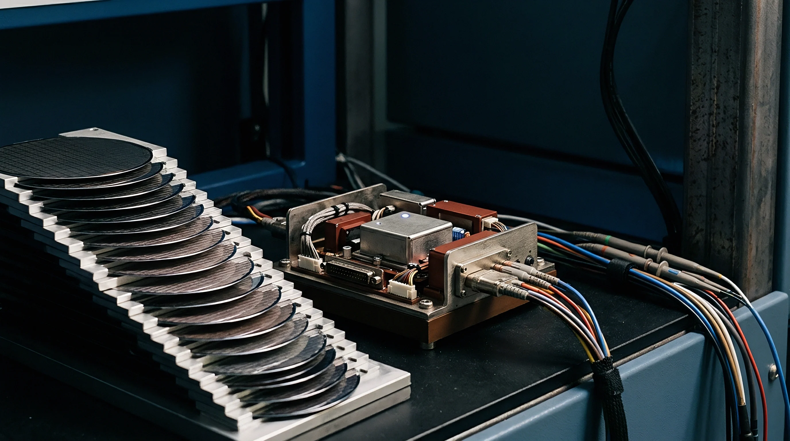
Coupling
When the final amplifier stage feeds energy back into the resonant tank, high-current synthesizers suffer severe electromagnetic pulling. Fundamental-frequency voltage-controlled oscillators are especially susceptible, since antenna mismatches bounce amplified RF power straight into the phase-locked loop inductors. If the phase of that reflection hits at the wrong angle, the oscillator injection-locks or jumps frequency by dozens of kilohertz.

Why Do Thermal Gradients Break Narrowband Locks?
A sharp temperature gradient across the quartz package destabilizes equivalent circuit parameters, moving the series resonant frequency faster than the phase-locked loop charge pump can correct phase error. Standard AT-cut or SC-cut blanks hold frequency well in stable ambient conditions, but a heat pulse on one edge of the ceramic package creates internal shear stress that momentarily distorts the crystal lattice spacing.
Synthesizer multiplication compounds these reference errors. A Fractional-N architecture stepping a thirty-two megahertz crystal up to eight hundred and sixty-eight megahertz or nine hundred and fifteen megahertz multiplies small quartz movements by twenty-seven or twenty-eight times. A transient reference shift of just ten hertz becomes a two hundred and eighty hertz offset at RF.
In a two-level FSK link with four-point-eight kilohertz deviation, an offset that large degrades symbol timing recovery and closes the demodulation eye pattern.
Synthesizer pulling reaches twenty-five kilohertz under a four-to-one voltage standing wave ratio when the transmitter stage delivers thirty decibel-milliwatts directly into an unbuffered fundamental oscillator tank.
Because varactor capacitance varies with voltage, VCO pulling during transmit bursts follows antenna load impedance closely. Compact internal antennas see heavy impedance shifts whenever hands, metal enclosures, or nearby objects move near the radiator. Without adequate reverse isolation between the power amplifier and local oscillator, this reflected energy pulls the center frequency mid-transmission.
| Output Power (dBm) | VCO Buffer Isolation (dB) | VSWR (All Phases) | Peak Frequency Slew (kHz) | Settling Duration (us) |
|---|---|---|---|---|
| +14 | 18 | 1.5:1 | 1.2 | 45 |
| +20 | 22 | 2.0:1 | 4.8 | 80 |
| +27 | 30 | 3.0:1 | 14.6 | 160 |
| +30 | 32 | 4.0:1 | 28.5 | 340 |
| +33 | 38 | 5.0:1 | 62.0 | 520 |
As load-induced offset drives up phase noise, prevention requires double-buffered distribution amplifiers between the VCO core and the high-power chain, alongside integrated cascode buffering inside the PLL silicon. Running the VCO at twice or four times the target carrier frequency ~ then dividing down to drive the mixer or pre-driver ~ prevents direct injection locking entirely. Isolating reference traces from high-current return paths must happen on the board before relying on firmware fixes.

Sink
On dense transceiver boards, thermal management dictates crystal frequency stability. Ground planes need to route heat away from sensitive timing circuits and toward chassis elements or structural sinks, rather than letting layout resistance dictate dissipation paths by accident.
Adding thermal relief trenches and copper cutouts between the amplifier and quartz oscillator establishes high-resistance barriers. Standard FR4 has an in-plane thermal conductivity of around zero-point-eight watts per meter-kelvin, while copper reaches nearly four hundred watts per meter-kelvin. Leaving unbroken copper pours beneath both the power amplifier and reference oscillator channels heat spikes straight into the quartz blank, triggering avoidable thermal drift during long transmissions.
Unbroken ground copper between high-power silicon and crystal oscillators transfers heat faster than natural board convection can dissipate it.
Because copper pours double as ground current paths, simple physical spacing is rarely enough without vertical and lateral thermal isolation structures built into the PCB stackup.
- Milling thermal isolation slots through inner and outer layers next to the amplifier ground paddle cuts thermal transfer toward reference oscillators by over twelve degrees Celsius per watt.
- Placing solid-filled copper thermal vias beneath the power transistor routes heat straight to bottom-layer cooling surfaces instead of spreading laterally across inner signal layers.
- Placing TCXOs on isolated PCB islands linked only by thin bridge traces dampens sudden conducted heat spikes.
- Fitting stamped copper RF shield cans over reference circuitry shields the quartz package from warm air plumes rising off hot matching components.
While shielding contains radiated RF fields, heat still moves inward through board traces. If these thermal channels stay unmanaged, carrier drift over a one-hundred-millisecond transmission can easily outrun the acquisition bandwidth of receiver baseband processors, causing total packet loss across industrial deployments.


Tracking
Digital baseband architectures use frequency estimation loops to handle whatever residual offset escapes physical board isolation. Modern sub-gigahertz transceivers pair open-loop compensation with closed-loop automatic frequency control to clean up static factory errors alongside dynamic thermal drift during incoming packet preambles.

Where Does Baseband Automatic Frequency Control Fail?
Rapid carrier slew can outpace discriminator integration windows, overflowing phase accumulators before the receiver locks frame sync. Standard AFC loops average phase differences across consecutive preamble symbols. When sudden PA heating curves frequency output quadratically or cubically over twenty symbols, that linear error estimator develops a severe systematic bias.
When the receiver mixer downconverts the signal in chirp spread spectrum systems like LoRa, any residual carrier offset turns into a timing error during de-chirping. Unchecked offset shifts the peak energy bin in the discrete Fourier transform array. If that shift exceeds twenty-five percent of the sub-carrier bandwidth, symbol error rates spike unless fine fractional-bin interpolation tracks the drift through the payload.
| Modulation Scheme | Signal Bandwidth (kHz) | Max Allowable CFO (kHz) | Demodulation Margin Loss (dB) | Typical CFO Limit (PPM) |
|---|---|---|---|---|
| 2-GFSK (BT=0.5) | 12.5 | 1.5 | 2.8 | 1.7 |
| 2-GFSK (BT=0.5) | 50.0 | 6.2 | 1.4 | 7.1 |
| 4-GFSK (BT=0.35) | 100.0 | 4.0 | 3.5 | 4.6 |
| LoRa (SF7) | 125.0 | 31.2 | 0.8 | 35.8 |
| LoRa (SF12) | 125.0 | 15.6 | 1.9 | 17.9 |
| SUN-OFDM (Opt 1) | 200.0 | 2.4 | 3.1 | 2.7 |
Because channel spacing sets tight error budgets, narrowband FSK requires careful preamble formatting so receiver loops can settle before payload data arrives. When initial thermal slew breaks phase lock early in the burst, extending preamble transmission gives the transmitter frequency time to stabilize before keying real data.
- Extended preamble sequences give receiving discriminators up to thirty-two alternating bit periods to calculate frequency offset before reading the sync word.
- Dual-stage frequency discriminators compute coarse offset over short correlation lags, then switch to longer windows for fine tracking.
- Baseband digital pre-distortion applies an inverse frequency ramp in transmitter firmware to neutralize expected thermal drift during initial RF pulses.
- Adaptive tracking loops tighten receiver filter bandwidths right after frame sync to keep phase noise from degrading payload reception.
If tight channel filters cut off drifting signal tails, the receiver drops the packet. Whether ultra-narrowband links can hold coherent lock through steep power ramps without dual-reference hardware remains an open engineering debate.

Penalty
Carrier offset hurts link budget by pushing signal energy into the attenuation skirts of channel selection filters. As a high-power transmitter wanders off center, IF filters clip modulated sidebands and degrade effective signal-to-noise ratio. Offsets reaching twenty percent of channel bandwidth impose an instant two to three decibel sensitivity penalty at the baseband detector.
That lost sensitivity cuts directly into operating range. In outdoor networks with a path loss exponent of three, dropping three decibels of link margin reduces working distance by more than twenty percent, severing marginal links without warning.
A three-decibel link margin degradation caused by transmitter carrier drift cuts usable communication coverage by one-fifth under typical ground propagation conditions.
Regulatory non-compliance is an equally sharp risk. Sub-gigahertz standards enforce strict frequency stability limits to prevent interference with adjacent channels, and regional regulators test spectral masks under full output power.
| Regulatory Standard | Frequency Band (MHz) | Conducted Limit (dBm) | Frequency Tolerance | Adjacent Band Rejection |
|---|---|---|---|---|
| ETSI EN 300 220-1 | 868.0 to 868.6 | +14 | 100 ppm | -30 dBc / 100 kHz |
| ETSI EN 300 220-2 | 869.4 to 869.65 | +27 | 10 ppm | -60 dBc / 25 kHz |
| FCC Part 15.247 | 902.0 to 928.0 | +30 | N/A (Mask Bounds) | -20 dBc / 100 kHz |
| FCC Part 90 (Narrow) | 450.0 to 470.0 | +33 | 1.5 ppm | Mask D (60 dBc) |
| ARIB STD-T108 | 920.6 to 923.4 | +13 | 20 ppm | -36 dBm / 100 kHz |
Meeting transmit spectral masks requires sharp out-of-band attenuation. If a power amplifier drifts by five kilohertz mid-burst, sideband skirts bleed across channel boundaries and fail type approval testing. Radiating thirty decibel-milliwatts in sub-gigahertz bands demands tight frequency lock throughout long packets to avoid adjacent-channel spill.
Section 4.2.3 of EN 300 220-1 caps instantaneous frequency error at twenty parts per million during transient transmission ~ meaning thermal slew that spills across power limits revokes certification outright.