Evaluating Flash Memory Execution Latency in Low Power Mesh Nodes
Execute-in-place NOR flash introduces bus wait states that erode radio timing guard bands during low-voltage battery pulse discharges.


Latch
Serial memory interfaces dictate microcontroller execution cadence during high-frequency radio events. When executing code directly from external SPI, Quad-SPI, or Octal-SPI NOR flash through Execute-in-Place, instruction fetch delays spill into system operation. Memory controllers fetch code in discrete 16- to 32-byte cache lines.
A cache hit lets the processor core run at its full clock frequency without wait states, but a cache miss halts execution while the controller issues command bytes, address phases, dummy cycles, and read requests across the physical bus.
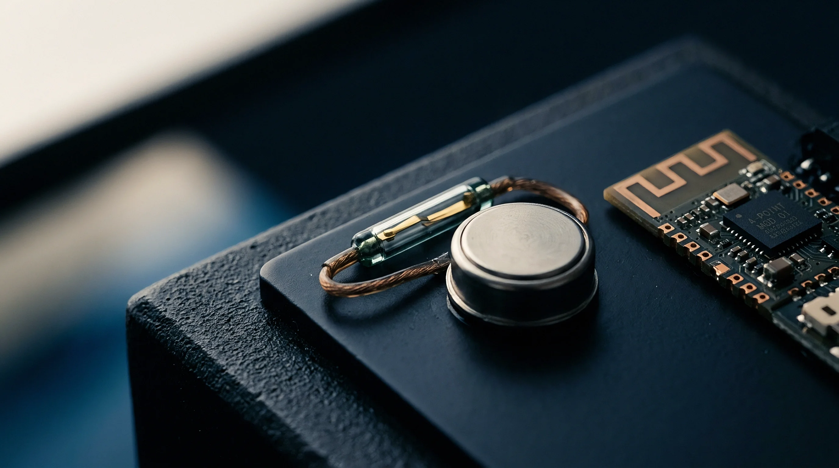
Instruction Fetch Architecture across Serial Memory Buses
Serial NOR memory devices use SPI protocol variants that trade pin count for bandwidth. Standard single-bit SPI takes eight clock cycles per byte, carrying a heavy fetch penalty. Quad-SPI uses four data lines, cutting transfer times by 75 percent.
Octal-SPI uses eight data lines and optional Double Data Rate signaling to move a byte on every clock edge. Trace capacitance, physical layout, and chip access times dictate the highest clock rates achievable in Execute-in-Place setups.
| Interface Type | Bus Clock Frequency | Command Overhead Cycles | Average Random Fetch Latency | Read Power Consumption |
|---|---|---|---|---|
| Standard SPI | 20 MHz | 32 cycles | 1.85 microseconds | 4.2 mA |
| Dual-SPI | 32 MHz | 24 cycles | 0.92 microseconds | 5.1 mA |
| Quad-SPI XiP | 48 MHz | 16 cycles | 0.43 microseconds | 7.8 mA |
| Octal-SPI DDR | 80 MHz | 8 cycles | 0.18 microseconds | 14.3 mA |
| On-Chip eFlash | 64 MHz | 0 cycles | 0.015 microseconds | 2.1 mA |

Hardware Flash Stall Mechanics
Instruction caching lowers average fetch latency but cannot prevent worst-case execution stalls. Linear code execution relies on prefetch buffers that speculatively load consecutive memory addresses, but unconditional branches, function calls, and hardware interrupt service routines force cache flushes that trigger blocking bus transactions.
- Bus turnaround cycles introduce fixed clock pauses whenever the controller toggles data lines from address output to byte reception.
- Cache line refills force the internal prefetch buffer to fetch 32 contiguous bytes, stalling instruction execution if code jumps across block boundaries.
- Internal charge-pump delays within serial NOR die delay page buffer reads following deep power-down recovery sequences.
- Concurrent flash write operations block read operations across the entire chip die unless dual-bank architecture exists.
Microcontrollers running complex radio protocol stacks see latency spikes whenever code paths branch into rarely accessed flash pages. A firmware routine constructing packet headers or running cryptographic algorithms can stall for dozens of clock cycles if the relevant memory blocks sit outside active cache buffers.
Quad-SPI NOR flash operating at 32 MHz introduces a 437-nanosecond fetch delay on every cache line miss during unaligned branch execution.
Peripheral bus stalls stem from physical wait-state cycles hardcoded into memory controller state machines, rather than unoptimized compiler flags.


Sag
Coin cell batteries exhibit sharp terminal voltage drops when radio power amplifiers energize. Primary lithium manganese dioxide cells retain an internal resistance between 15 and 30 ohms at room temperature, rising past 100 ohms near end-of-life or below freezing conditions. Drawing a 15 mA transmit pulse from a fresh cell drops terminal voltage from 3.0V to 2.55V instantly.
Concurrent activation of serial flash charge pumps during erase or program operations pulls additional current spikes, driving supply voltage toward the brown-out reset threshold.

Supply Voltage Scaling and NOR Flash Access Margins
Serial flash access times degrade as supply voltage drops. At 3.3V, a standard Quad-SPI NOR memory die achieves 104 MHz clock frequencies with four dummy cycles. Operating that same die at 1.8V extends transistor switching delays inside row decoders and sense amplifiers, forcing the memory controller to dynamically insert extra wait states or downscale the bus clock frequency to prevent data corruption.
| Supply Rail Voltage | PA Transmit Current | Flash Clock Limit | Mandatory Read Wait States | Measured Latency Penalty |
|---|---|---|---|---|
| 3.3V | 12.1 mA | 104 MHz | 4 cycles | 0.00 us |
| 2.7V | 13.8 mA | 80 MHz | 6 cycles | 0.12 us |
| 2.2V | 16.5 mA | 48 MHz | 8 cycles | 0.38 us |
| 1.8V | 19.2 mA | 32 MHz | 10 cycles | 0.74 us |
When supply voltage drops to 1.8V, internal sensing margins within flash cells shrink, requiring longer integration times for read amplifiers to distinguish programmed states from erased states.
Dynamic clock downscaling protects serial memory against read corruption during radio power amplifier current spikes at low supply voltages.

Thermal and Charge Pump Drift
Low temperatures increase the viscosity of electrolyte formulations inside primary batteries, compounding supply sag during radio activity. NOR flash memory chips rely on internal charge pumps to generate high bias voltages for word-line gating and array sensing. At sub-zero temperatures, charge pump efficiency declines, lengthening internal voltage stabilization routines after power-up from deep sleep modes.
Firmware executing directly from flash faces variable execution timing depending on ambient temperature and battery charge state.
Ignoring the voltage drop induced by concurrent radio transmission and flash read operations produces unrecoverable bus timing faults that reset the microcontroller during node join procedures.

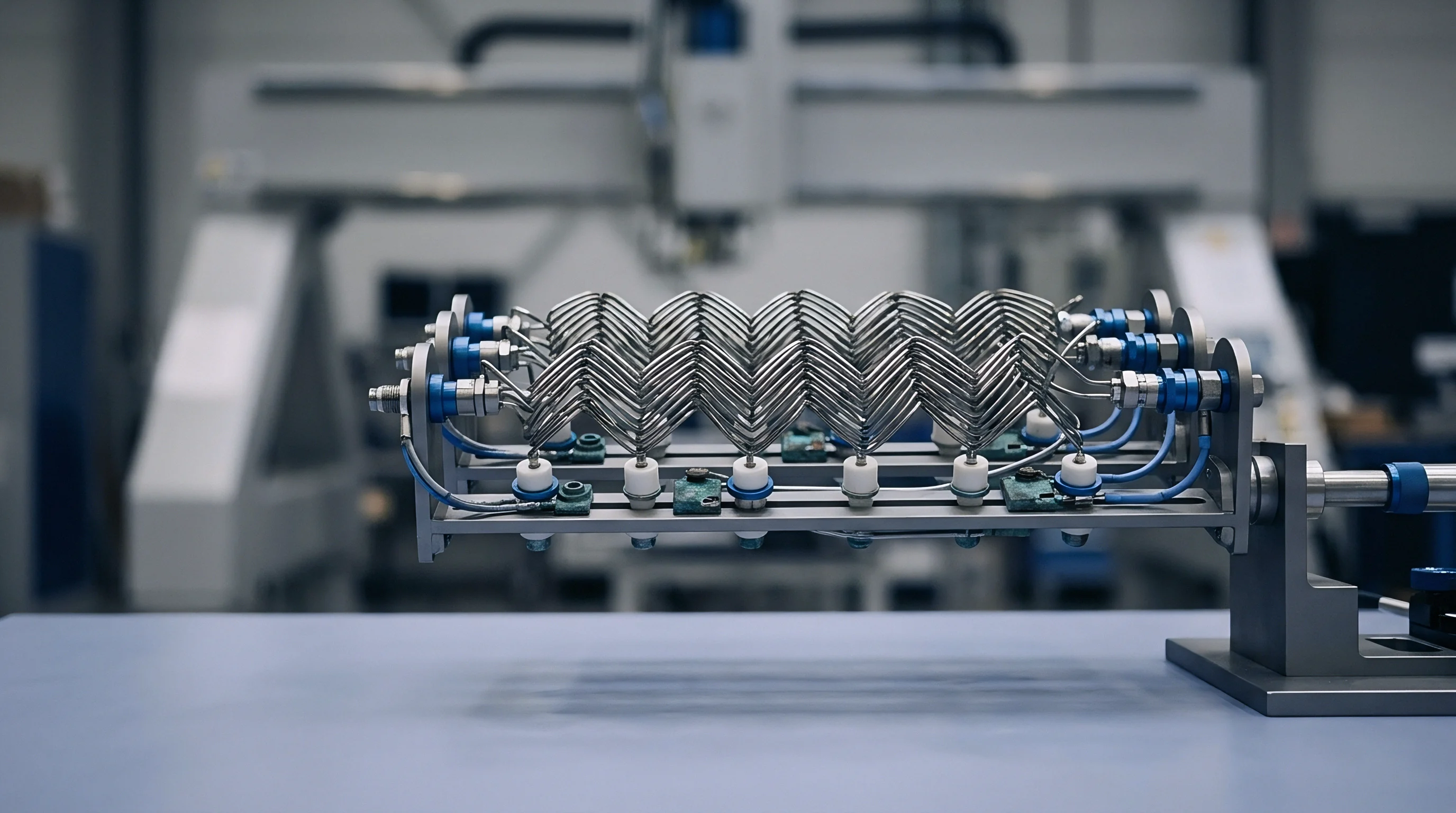
Slot
Time-synchronized wireless protocol frames require deterministic processing windows. Time-Slotted Channel Hopping architectures divide time into precise periodic slots, typically 10 to 15 milliseconds long. Within each slot, a node must wake from deep sleep, tune its RF transceiver to the designated channel, construct the packet payload, transmit the frame, switch to receive mode, and capture the incoming acknowledgment packet.
Guard time allocations limit acceptable timing drift to narrow windows, frequently set to plus or minus 50 microseconds.
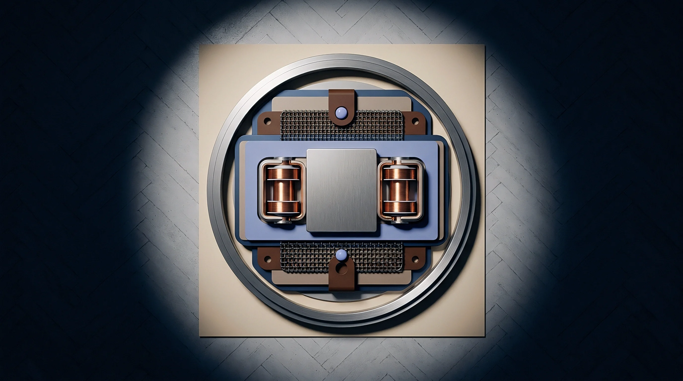
Time Slotted Channel Hopping Guard Band Erosion
Instruction execution delays from flash wait states alter packet framing mechanics. When an incoming radio interrupt wakes the CPU, the core must execute interrupt vector preambles, restore register contexts, and load radio driver instructions. If these code segments reside in serial NOR memory, cache misses delay CPU response time.
IEEE 802.15.4-2020 specifies maximum clock drift tolerances that cause immediate link desynchronization if instruction fetch delays push transmission timing beyond the defined guard interval.
If execution delays cause packet assembly to exceed the guard time boundary, the transmission starts late, missing the receiving node listen window entirely.
- Critical vector placement locates time-sensitive interrupt routines inside high-speed zero-wait-state internal SRAM rather than external serial memory.
- Direct memory access configuration bypasses CPU memory buses by streaming incoming radio packet payload directly to peripheral RAM buffers.
- Pre-fetch buffer activation keeps the instruction cache warm prior to predictable radio timer expiry events across synchronization cycles.
- Dual-bank flash isolation allocates firmware updates to a secondary bank while the active stack executes without read stalls from primary memory.
Section 6.5.3 of the IEEE 802.15.4 specification limits frame transmission delay jitter, forcing hardware designers to guarantee deterministic execution bounds under peak memory access loads.


Bench
Quantifying instruction fetch delay requires direct pin observation under active radio workloads. Measuring average latency through firmware timing loops introduces measurement overhead that masks microsecond-level cache miss stalls. Test benches utilize high-speed logic analyzers clipped to Quad-SPI bus lines combined with current probes connected to microcontroller power supply rails.

How Does Trace Hardware Capture Interrupt Timing Overhead?
Embedded trace macrocells output instruction execution metrics in real time without halting CPU cores. By monitoring hardware signals corresponding to interrupt request lines and serial memory chip-select outputs, test equipment measures the exact elapsed time between interrupt assertion and the first instruction fetch cycle.
High-precision optical time-domain reflectometry in fiber infrastructure relies on similar sub-nanosecond pulse tagging to isolate structural breaks across distant physical media.
Trace channels capture pin states during active signal transitions.
- Connect logic analyzer channels to the Quad-SPI chip select, clock, and data lines while attaching a current probe to the microcontroller supply line.
- Trigger trace capture on the rising edge of the radio software interrupt line preceding packet payload assembly.
- Measure the time delta between interrupt assertion and the first Quad-SPI read command byte issued by the memory controller.
- Calculate the total wait-state latency by comparing actual clock cycles spent in data retrieval against theoretical zero-wait SRAM instruction fetch timing.
Whether hardware prefetch mechanisms can entirely eliminate worst-case instruction fetch jitter across non-deterministic mesh routing paths remains an open question.


Tariff
Silicon fabrication nodes dictate whether microcontrollers integrate internal memory dies or rely on serial interfaces. Microcontrollers fabricated on mature 90nm or 40nm process technologies cost-effectively integrate embedded flash directly onto the logic die, eliminating external serial bus latency. Advanced semiconductor nodes at 28nm and sub-22nm planar architectures lack cost-effective embedded flash options due to mask complexity and leakage current challenges.
Designers choosing modern low-power microcontrollers operating on advanced nodes must accept external serial memory or co-packaged System-in-Package silicon dies.

Silicon Process Constraints and Memory Sourcing Arithmetic
System-in-Package integration combines a microcontroller logic die and a serial NOR flash die inside a single plastic package. This approach eliminates circuit board routing complexity while maintaining physical Quad-SPI or Octal-SPI interfaces internally. Silicon yields drop at sub-28nm.
Die area dictates module cost. Module pricing reflects both component costs and assembly yields.
| Memory Architecture | Process Node | Module Unit Cost | Execution Latency | Assembly Complexity |
|---|---|---|---|---|
| On-Chip eFlash | 40nm | $2.85 | 15 nanoseconds | Low |
| Co-Packaged SiP NOR | 28nm | $2.10 | 180 nanoseconds | Medium |
| External QSPI NOR | 22nm | $1.65 | 430 nanoseconds | High |
| External Octal-SPI | 22nm | $1.95 | 180 nanoseconds | High |
Modern 22nm microcontrollers achieve lower sleep currents and lower logic cost, but external flash interface timing offsets a portion of those operational gains.
External serial memory selection shifts system cost from silicon fabrication fees to assembly yield risk and testing complexity.
Selecting external serial flash for low-power mesh nodes requires balancing the lower upfront chip price against the permanent power budget penalty of bus fetch overhead.