Meaning
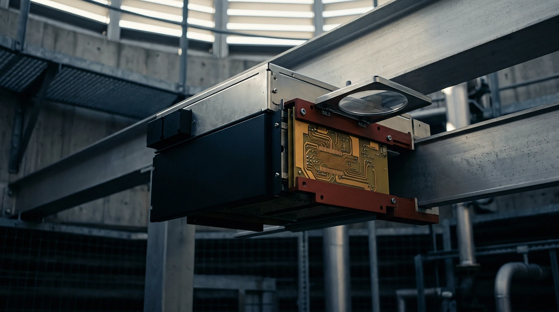
The geometric configuration of conductive paths on a printed circuit board establishes the physical connections between integrated circuits and discrete components. Through meticulous board trace routing, designers define the width, spacing, and path of high-frequency transmission lines. This process determines the susceptibility of the system to electromagnetic interference and signal degradation.
Modern routing techniques prioritize direct paths and minimize the use of vias in high-speed lanes.
Signal Integrity
Crosstalk between adjacent parallel lines is a primary risk when digital transitions occur at high speeds. The physical spacing chosen during board trace routing determines the degree of capacitive and inductive coupling. Wide gaps reduce these unwanted interactions but increase the required board area.
Engineers use guard traces or ground planes to isolate sensitive analogue paths from noisy digital lines.
Impedance Control
Consistent line widths must be maintained across the entire path to prevent reflections that distort the digital pulse. When board trace routing introduces sudden turns or transitions between layers, it creates localized impedance discontinuities that degrade performance. Rounded corners or forty-five-degree bends are preferred to sharp right-angle turns.
Manufacturing Tolerance
Fabrication limitations constrain the minimum width and gap of the copper paths. Production yields decrease when the routing requires geometries that approach the capability limit of the plating process. Consequently, practical designs employ conservative rules that align with standard fabrication tolerances.